SNVSA30A March   2015  – October 2016 LM36923

PRODUCTION DATA.  

  1. Features
  2. Applications
  3. Description
  4. Revision History
  5. Pin Configuration and Functions
  6. Specifications
    1. 6.1 Absolute Maximum Ratings
    2. 6.2 ESD Ratings
    3. 6.3 Recommended Operating Conditions
    4. 6.4 Thermal Information
    5. 6.5 Electrical Characteristics
    6. 6.6 I2C Timing Requirements
    7. 6.7 Typical Characteristics
  7. Detailed Description
    1. 7.1 Overview
    2. 7.2 Functional Block Diagram
    3. 7.3 Feature Description
      1. 7.3.1 Enabling the LM36923
        1. 7.3.1.1 Current Sink Enable
      2. 7.3.2 LM36923 Start-Up
      3. 7.3.3 Brightness Mapping
        1. 7.3.3.1 Linear Mapping
        2. 7.3.3.2 Exponential Mapping
      4. 7.3.4 PWM Input
        1. 7.3.4.1 PWM Sample Frequency
          1. 7.3.4.1.1 PWM Resolution and Input Frequency Range
          2. 7.3.4.1.2 PWM Sample Rate and Efficiency
            1. 7.3.4.1.2.1 PWM Sample Rate Example
        2. 7.3.4.2 PWM Hysteresis
        3. 7.3.4.3 PWM Step Response
        4. 7.3.4.4 PWM Timeout
      5. 7.3.5 LED Current Ramping
      6. 7.3.6 Regulated Headroom Voltage
    4. 7.4 Device Functional Modes
      1. 7.4.1 Brightness Control Modes
        1. 7.4.1.1 I2C Only (Brightness Mode 00)
        2. 7.4.1.2 PWM Only (Brightness Mode 01)
        3. 7.4.1.3 I2C + PWM Brightness Control (Multiply Then Ramp) Brightness Mode 10
        4. 7.4.1.4 I2C + PWM Brightness Control (Ramp Then Multiply) Brightness Mode 11
      2. 7.4.2 Boost Switching Frequency
        1. 7.4.2.1 Minimum Inductor Select
      3. 7.4.3 Auto Switching Frequency
      4. 7.4.4 Backlight Adjust Input (BL_ADJ)
        1. 7.4.4.1 Back-Light Adjust Input Polarity
      5. 7.4.5 Fault Protection/Detection
        1. 7.4.5.1 Overvoltage Protection (OVP)
          1. 7.4.5.1.1 Case 1 OVP Fault Only (OVP Threshold Hit and All Enabled Current Sink Inputs > 40 mV)
          2. 7.4.5.1.2 Case 2a OVP Fault and Open LED String Fault (OVP Threshold Occurrence and Any Enabled Current Sink Input ≤ 40 mV)
          3. 7.4.5.1.3 Case 2b OVP Fault and Open LED String Fault (OVP Threshold Duration and Any Enabled Current Sink Input ≤ 40 mV)
          4. 7.4.5.1.4 OVP/LED Open Fault Shutdown
          5. 7.4.5.1.5 Testing for LED String Open
        2. 7.4.5.2 LED String Short Fault
        3. 7.4.5.3 Overcurrent Protection (OCP)
          1. 7.4.5.3.1 OCP Fault
          2. 7.4.5.3.2 OCP Shutdown
        4. 7.4.5.4 Device Overtemperature (TSD)
          1. 7.4.5.4.1 Overtemperature Shutdown
    5. 7.5 Programming
      1. 7.5.1 I2C Interface
        1. 7.5.1.1 Start and Stop Conditions
        2. 7.5.1.2 I2C Address
        3. 7.5.1.3 Transferring Data
        4. 7.5.1.4 Register Programming
    6. 7.6 Register Maps
  8. Applications and Implementation
    1. 8.1 Application Information
    2. 8.2 Typical Application
      1. 8.2.1 Design Requirements
      2. 8.2.2 Detailed Design Procedure
        1. 8.2.2.1 Component Selection
          1. 8.2.2.1.1 Inductor
          2. 8.2.2.1.2 Output Capacitor
          3. 8.2.2.1.3 Input Capacitor
      3. 8.2.3 Application Curves
  9. Power Supply Recommendations
    1. 9.1 Input Supply Bypassing
  10. 10Layout
    1. 10.1 Layout Guidelines
      1. 10.1.1 Boost Output Capacitor Placement
      2. 10.1.2 Schottky Diode Placement
      3. 10.1.3 Inductor Placement
      4. 10.1.4 Boost Input Capacitor Placement
    2. 10.2 Layout Example
  11. 11Device and Documentation Support
    1. 11.1 Device Support
      1. 11.1.1 Third-Party Products Disclaimer
    2. 11.2 Receiving Notification of Documentation Updates
    3. 11.3 Community Resources
    4. 11.4 Trademarks
    5. 11.5 Electrostatic Discharge Caution
    6. 11.6 Glossary
  12. 12Mechanical, Packaging, and Orderable Information

Package Options

Mechanical Data (Package|Pins)
Thermal pad, mechanical data (Package|Pins)
Orderable Information

5 Pin Configuration and Functions

YFF Package
12-Pin DSBGA
Top View
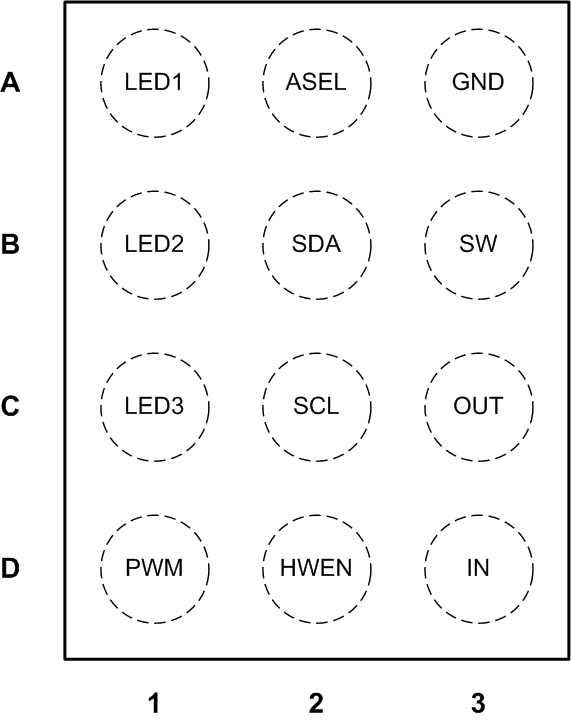
LM36923 pin_diagram_23.gif

Pin Functions

PIN I/O DESCRIPTION
NUMBER NAME
A1 LED1 Input Input to current sink 1. The boost converter regulates the minimum voltage between LED1, LED2, LED3 to VHR.
A2 BL_ADJ Input LED current adjust input. When BL_ADJ is driven to a logic high voltage the LED current steps down to the programmed low current value.
A3 GND Input Ground
B1 LED2 Input Input pin to current sink 2. The boost converter regulates the minimum voltage between LED1, LED2 ,LED3 to VHR.
B2 SDA I/O Data I/O for I2C-Compatible Interface.
B3 SW Output Drain Connection for internal low side NFET, and anode connection for external Schottky diode.
C1 LED3 Input Input pin to current sink 3. The boost converter regulates the minimum voltage between LED1, LED2, LED3 to VHR.
C2 SCL Input Clock Input for I2C-compatible interface.
C3 OUT Input OUT serves as the sense point for overvoltage protection. Connect OUT to the positive pin of the output capacitor.
D1 PWM Input Logic level input for PWM current control.
D2 HWEN Input Hardware enable input. Drive HWEN high to bring the device out of shutdown and allow I2C writes or PWM control.
D3 IN Input Input voltage connection. Bypass IN to GND with a minimum 2.2-µF ceramic capacitor.