SNOSCS2D November   2013  – March 2019 LM3697

PRODUCTION DATA.  

  1. Features
  2. Applications
  3. Description
    1.     Device Images
      1.      Simplified Schematic
      2.      Boost Efficiency
  4. Revision History
  5. Pin Configuration and Functions
    1.     Pin Functions
  6. Specifications
    1. 6.1 Absolute Maximum Ratings
    2. 6.2 ESD Ratings
    3. 6.3 Recommended Operating Conditions
    4. 6.4 Thermal Information
    5. 6.5 Electrical Characteristics
    6. 6.6 Timing Requirements
    7. 6.7 Typical Characteristics
  7. Detailed Description
    1. 7.1 Overview
      1. 7.1.1 PWM Input
      2. 7.1.2 HWEN Input
      3. 7.1.3 Thermal Shutdown
    2. 7.2 Functional Block Diagram
    3. 7.3 Feature Descriptions
      1. 7.3.1 High-Voltage LED Control
        1. 7.3.1.1 High-Voltage Boost Converter
        2. 7.3.1.2 High-Voltage Current Sinks (HVLED1, HVLED2 and HVLED3)
        3. 7.3.1.3 High-Voltage Current String Biasing
      2. 7.3.2 Boost Switching-Frequency Select
      3. 7.3.3 Automatic Switching Frequency Shift
      4. 7.3.4 Brightness Register Current Control
        1. 7.3.4.1 8-Bit Control (Preferred)
        2. 7.3.4.2 11-Bit Control
      5. 7.3.5 PWM Control
        1. 7.3.5.1 PWM Input Frequency Range
        2. 7.3.5.2 PWM Input Polarity
        3. 7.3.5.3 PWM Zero Detection
      6. 7.3.6 Start-up/Shutdown Ramp
      7. 7.3.7 Run-Time Ramp
      8. 7.3.8 High-Voltage Control A and B Ramp Select
    4. 7.4 Device Functional Modes
      1. 7.4.1 LED Current Mapping Modes
        1. 7.4.1.1 Exponential Mapping
          1. 7.4.1.1.1 8-Bit Code Calculation
          2. 7.4.1.1.2 11-Bit Code Calculation
        2. 7.4.1.2 Linear Mapping
          1. 7.4.1.2.1 8-Bit Code Calculation
          2. 7.4.1.2.2 11-Bit Code Calculation
      2. 7.4.2 Fault Flags/Protection Features
        1. 7.4.2.1 Open LED String (HVLED)
        2. 7.4.2.2 Shorted LED String (HVLED)
        3. 7.4.2.3 Overvoltage Protection (Inductive Boost)
        4. 7.4.2.4 Current Limit (Inductive Boost)
      3. 7.4.3 I2C-Compatible Interface
        1. 7.4.3.1 Start And Stop Conditions
        2. 7.4.3.2 I2C-Compatible Address
        3. 7.4.3.3 Transferring Data
        4. 7.4.3.4 High-Speed Mode
    5. 7.5 Register Maps
  8. Application and Implementation
    1. 8.1 Application Information
    2. 8.2 Typical Applications
      1. 8.2.1 Design Requirements
      2. 8.2.2 Detailed Design Procedure
        1. 8.2.2.1 Boost Converter Maximum Output Power
          1. 8.2.2.1.1 Peak Current Limited
          2. 8.2.2.1.2 Output Voltage Limited
        2. 8.2.2.2 Inductor Selection
        3. 8.2.2.3 Output Capacitor Selection
        4. 8.2.2.4 Schottky Diode Selection
        5. 8.2.2.5 Input Capacitor Selection
        6. 8.2.2.6 Application Circuit Component List
      3. 8.2.3 Application Performance Plots
    3. 8.3 Initialization Set Up
  9. Power Supply Recommendations
  10. 10Layout
    1. 10.1 Layout Guidelines
      1. 10.1.1 Boost Output Capacitor Placement
      2. 10.1.2 Schottky Diode Placement
      3. 10.1.3 Inductor Placement
      4. 10.1.4 Boost Input Capacitor Placement
    2. 10.2 Layout Example
  11. 11Device and Documentation Support
    1. 11.1 Device Support
      1. 11.1.1 Third-Party Products Disclaimer
    2. 11.2 Related Documentation
    3. 11.3 Receiving Notification of Documentation Updates
    4. 11.4 Community Resources
    5. 11.5 Trademarks
    6. 11.6 Electrostatic Discharge Caution
    7. 11.7 Glossary
  12. 12Mechanical, Packaging, and Orderable Information

Package Options

Refer to the PDF data sheet for device specific package drawings

Mechanical Data (Package|Pins)
  • YFQ|12
Thermal pad, mechanical data (Package|Pins)
Orderable Information

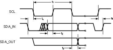
Timing Requirements

MIN NOM MAX UNIT
I2C-COMPATIBLE TIMING SPECIFICATIONS (SCL, SDA)(1)
t1 SCL (clock period) 2.7 V ≤ VIN ≤ 5.5 V 2.5 µs
t2 Data In set-up time to SCL high 2.7 V ≤ VIN ≤ 5.5 V 100 ns
t3 Data out stable after SCL low 2.7 V ≤ VIN ≤ 5.5 V 0 ns
t4 SDA low set-up time to SCL low (start) 2.7 V ≤ VIN ≤ 5.5 V 100 ns
t5 SDA high hold time after SCL high (stop) 2.7 V ≤ VIN ≤ 5.5 V 100 ns
INTERNAL POR THRESHOLD AND HWEN TIMING SPECIFICATION
VPOR POR reset release voltage threshold VIN ramp time = 100 µs 1.7 2.1 V
VIN ramp time = 100 µs, TA = 25°C 1.9
tHWEN First I2C start pulse after HWEN high 2.7 V ≤ VIN ≤ 5.5 V, POR reset complete 20 µs
POR reset complete, TA = 25°C 5.0
SCL and SDA must be glitch-free in order for proper brightness control to be realized.
LM3697 30200389.gifFigure 1. I2C-Compatible Interface Timing