SNOS455G May 2000 – September 2015 LM4050-N , LM4050-N-Q1
PRODUCTION DATA.
- 1 Features
- 2 Applications
- 3 Description
- 4 Revision History
- 5 Pin Configuration and Functions
-
6 Specifications
- 6.1 Absolute Maximum Ratings
- 6.2 ESD Ratings
- 6.3 Recommended Operating Conditions
- 6.4 Thermal Information
- 6.5 Electrical Characteristics: 2-V Option
- 6.6 Electrical Characteristics: 2.5-V Option
- 6.7 Electrical Characteristics: 4.1-V Option
- 6.8 Electrical Characteristics: 5-V Option
- 6.9 Electrical Characteristics: 8.2-V Option
- 6.10 Electrical Characteristics: 10-V Option
- 6.11 Typical Characteristics
- 7 Parameter Measurement Information
- 8 Detailed Description
- 9 Application and Implementation
- 10Power Supply Recommendations
- 11Layout
- 12Device and Documentation Support
- 13Mechanical, Packaging, and Orderable Information
Package Options
Mechanical Data (Package|Pins)
- DBZ|3
Thermal pad, mechanical data (Package|Pins)
Orderable Information
9 Application and Implementation
NOTE
Information in the following applications sections is not part of the TI component specification, and TI does not warrant its accuracy or completeness. TI’s customers are responsible for determining suitability of components for their purposes. Customers should validate and test their design implementation to confirm system functionality.
9.1 Application Information
The LM4050-N is a precision micropower curvature-corrected bandgap shunt voltage reference. For space critical applications, the LM4050-N is available in the sub-miniature SOT-23 surface-mount package. The LM4050-N has been designed for stable operation without the need of an external capacitor connected between the + pin and the − pin. If, however, a bypass capacitor is used, the LM4050-N remains stable. Reducing design effort is the availability of several fixed reverse breakdown voltages: 2.048 V, 2.5 V, 4.096 V, 5 V, 8.192 V, and 10 V. The minimum operating current increases from 60 μA for the LM4050-N-2.0 to 100 μA for the LM4050-N-10.0. All versions have a maximum operating current of 15 mA.
LM4050-Ns in the SOT-23 packages have a parasitic Schottky diode between pin 2 (−) and pin 3 (Die attach interface contact). Therefore, pin 3 of the SOT-23 package must be left floating or connected to pin 2.
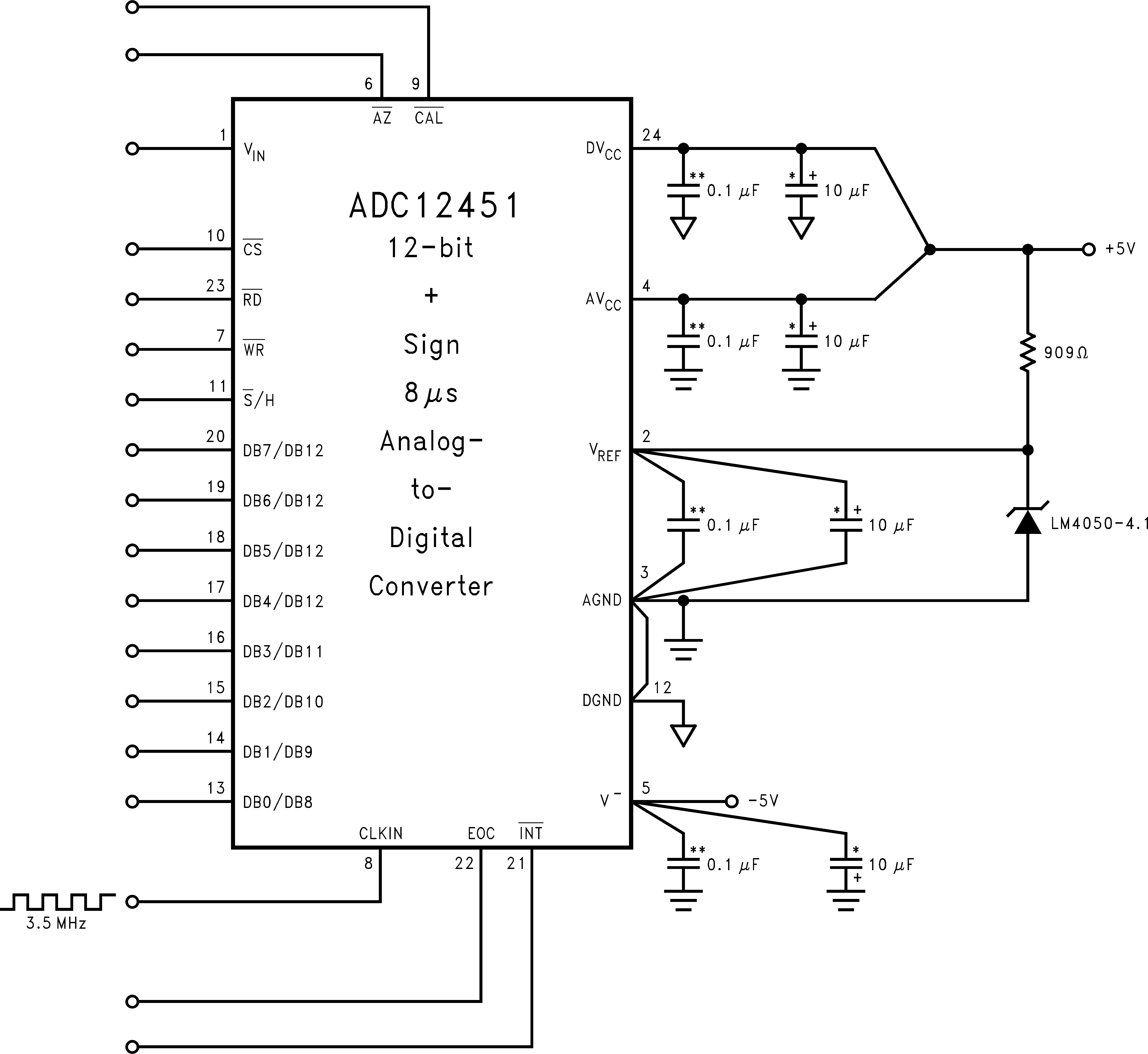
The 4.096-V version allows single 5-V 12-bit ADCs or DACs to operate with an LSB equal to 1 mV. For 12-bit ADCs or DACs that operate on supplies of 10 V or greater, the 8.192-V version gives 2 mV per LSB.
The typical thermal hysteresis specification is defined as the change in 25°C voltage measured after thermal cycling. The device is thermal cycled to temperature –40°C and then measured at 25°C. Next the device is thermal cycled to temperature 125°C and again measured at 25°C. The resulting VOUT delta shift between the 25°C measurements is thermal hysteresis. Thermal hysteresis is common in precision references and is induced by thermal-mechanical package stress. Changes in environmental storage temperature, operating temperature and board mounting temperature are all factors that can contribute to thermal hysteresis.
In a conventional shunt regulator application (Figure 10) , an external series resistor (RS) is connected between the supply voltage and the LM4050-N. RS determines the current that flows through the load (IL) and the LM4050-N (IQ). Since load current and supply voltage may vary, RS should be small enough to supply at least the maximum guaranteed IRMIN (spec. table) to the LM4050-N even when the supply voltage is at its minimum and the load current is at its maximum value. When the supply voltage is at its maximum and IL is at its minimum, RS should be large enough so that the current flowing through the LM4050-N is less than 15 mA.
RS is determined by the supply voltage, (VS), the load and operating current, (IL and IQ), and the LM4050-N's reverse breakdown voltage, VR.

9.2 Typical Applications
9.2.1 Shunt Regulator
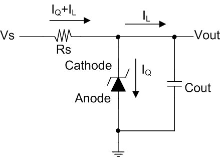 Figure 10. Shunt Regulator Schematic
9.2.1.1 Design Requirements
For this design example, use the parameters listed in Table 1 as the input parameters.
Table 1. Design Parameters
| DESIGN PARAMETER | VALUE |
|---|---|
| Output Voltage | 2 V, 2.5 V, 4.1 V, 5 V, 8.2 V, 10 V |
| Minimum Cathode Current | 41 µA, 41 µA, 52 µA, 56 µA, 74 µA, 80 µA (Typical) (Respective to Above field) |
9.2.1.2 Detailed Design Procedure
RS sets the cathode current of the shunt reference. Ensure that this current is greater than the minimum cathode current to ensure regulation and less that the maximum reverse current to prevent overheating of the shunt reference. A suggested good starting value for most designs is from approximately 0.5 mA to 1 mA.

9.2.1.3 Application Curve
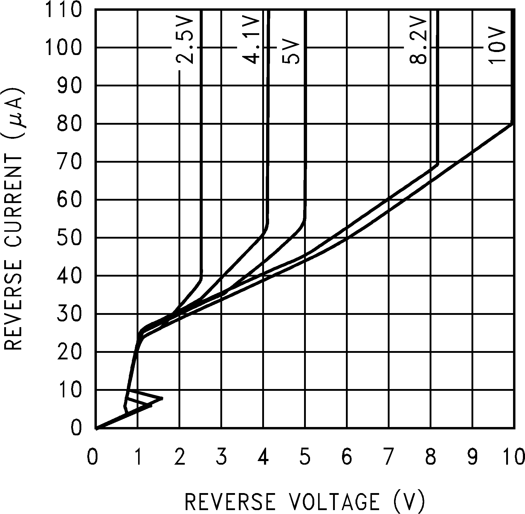 Figure 11. Reverse Characteristics and Minimum Operating Current
9.2.2 Precision Reference for an Analog-to-Digital Converter
*Tantalum
9.2.2.1 Design Requirements
For this design example, use the parameters listed in Table 2 as the input parameters.
Table 2. Design Parameters
| DESIGN PARAMETER | VALUE |
|---|---|
| Output Voltage | 4.1 V |
9.2.2.2 Detailed Design Procedure
Set IQ to approximately 1 mA.

where
- Rs = 900 Ω, nearest preferred Value = 909 Ω
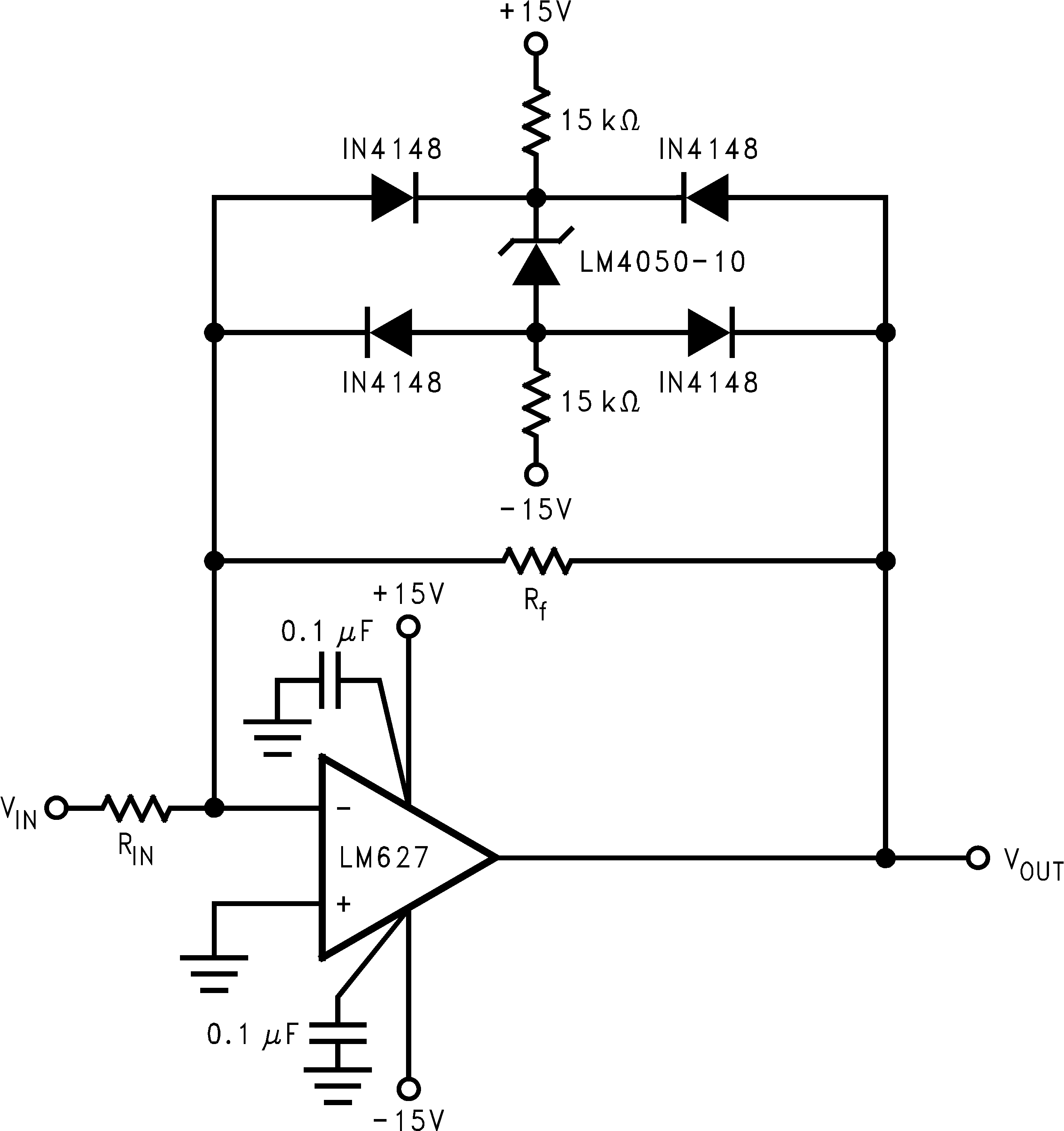
9.2.3 VOUT Bounded Amplifier
9.2.3.1 Design Requirements
The only design requirement is VOUT bounded to ±11.5 V.
9.2.3.2 Detailed Design Procedure


Set IQ to approximately 0.6 mA.


where
- RS (total) = 33 kΩ (select 2 × 15 kΩ)
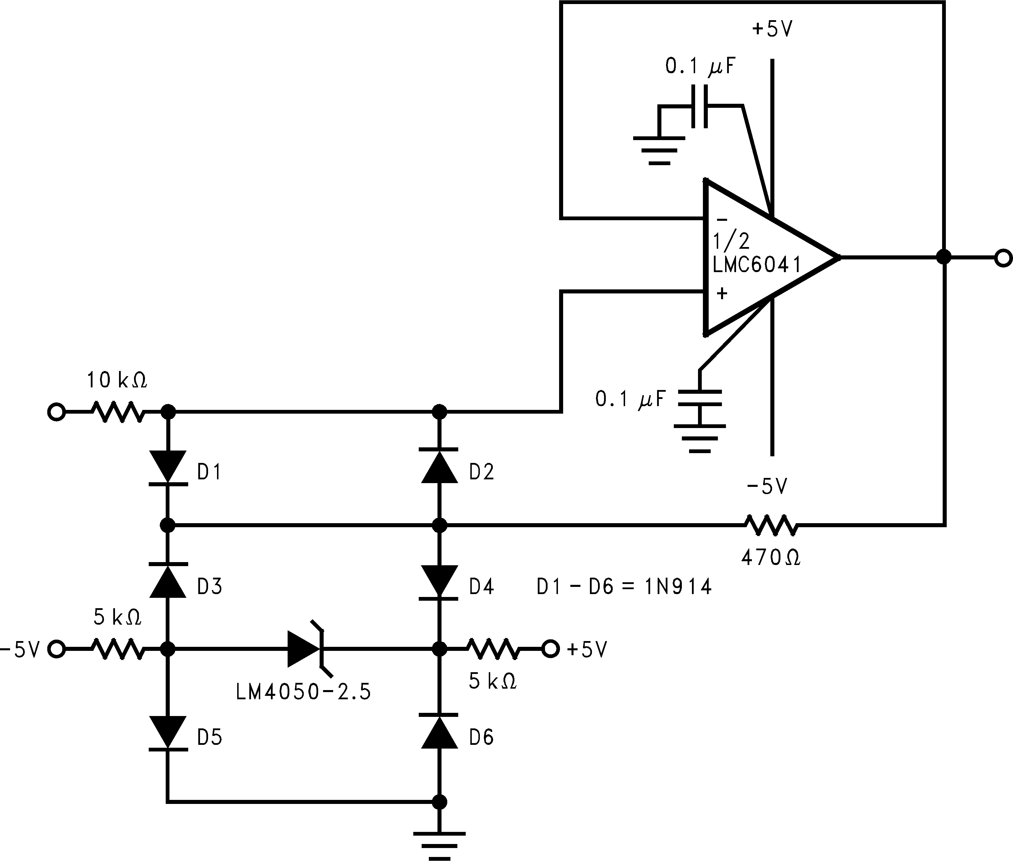
9.2.4 VIN Bounded Amplifier
9.2.4.1 Design Requirements
The only design requirement is VIN bounded to ±4.6 V.
9.2.4.2 Detailed Design Procedure


Set IQ to approximately 0.6 mA.


where
- RS (total) = 12.5 kΩ (select 2 × 5 kΩ)
9.2.5 ±4.096 Precision Reference
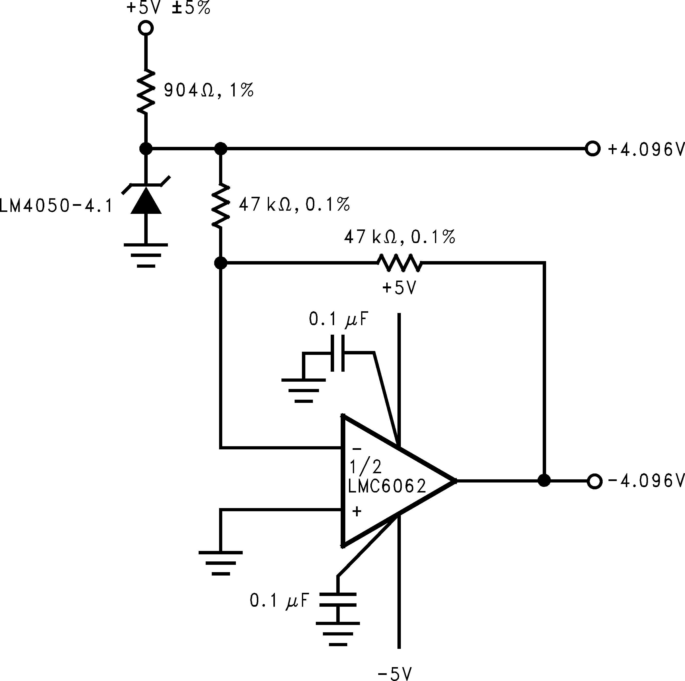 Figure 15. Precision ±4.096v Reference
9.2.5.1 Design Requirements
The only design requirement is a positive and negative reference generated from a positive reference, ±4.096 V.
9.2.5.2 Detailed Design Procedure
Follow the design procedure set in Precision Reference for an Analog-to-Digital Converter.
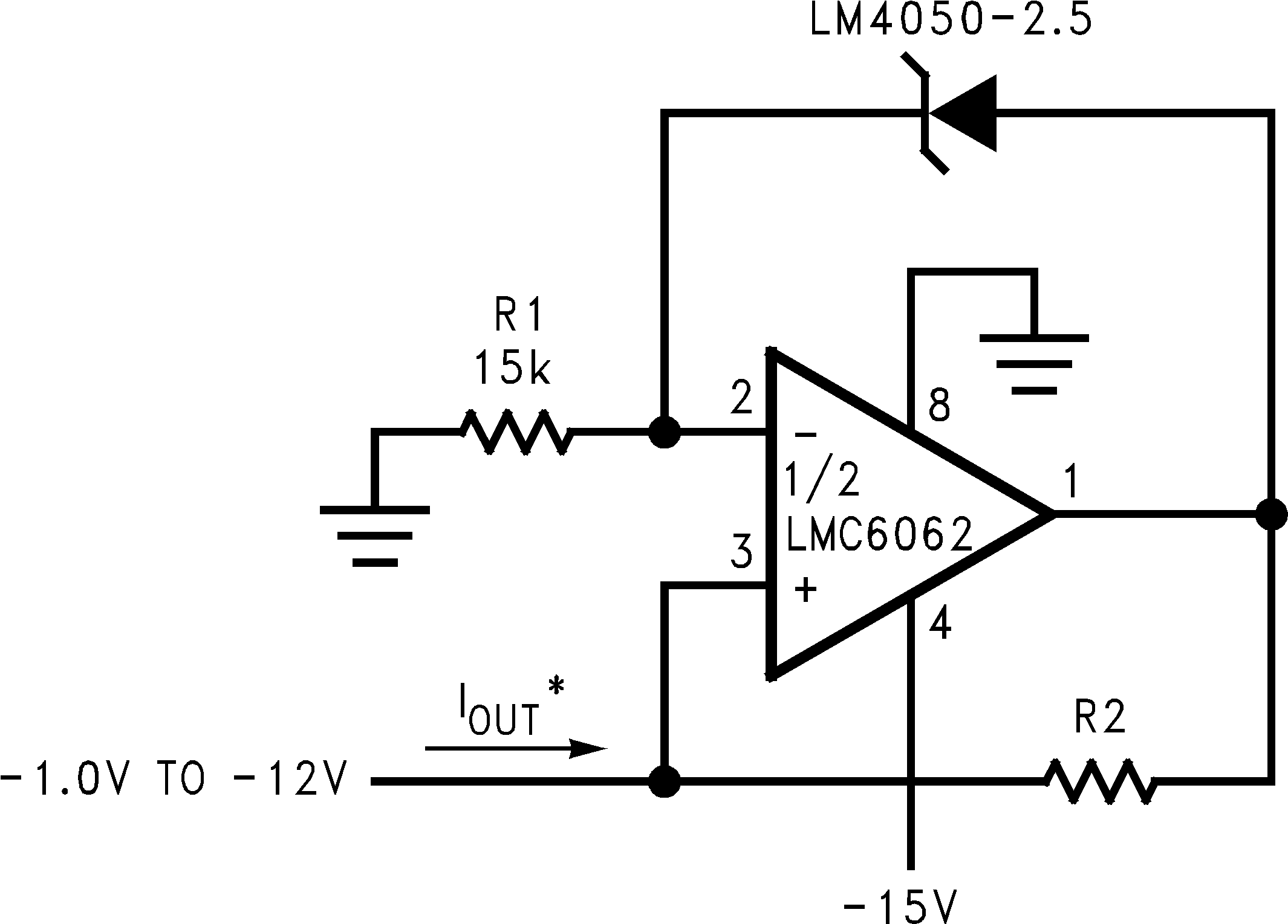
9.2.6 ±1-mA Precision Current Sources
9.2.6.1 Design Requirements
The only design requirement is a dual ±1-mA current source.
9.2.6.2 Detailed Design Procedure
Set worse-case cathode current to 0.6 mA.


