SNVS788H January 2012 – August 2021 LM5019
PRODUCTION DATA
- 1 Features
- 2 Applications
- 3 Description
- 4 Revision History
- 5 Pin Configuration and Functions
- 6 Specifications
-
7 Detailed Description
- 7.1 Overview
- 7.2 Functional Block Diagram
- 7.3
Feature Description
- 7.3.1 Control Overview
- 7.3.2 VCC Regulator
- 7.3.3 Regulation Comparator
- 7.3.4 Overvoltage Comparator
- 7.3.5 On-Time Generator
- 7.3.6 Current Limit
- 7.3.7 N-Channel Buck Switch and Driver
- 7.3.8 Synchronous Rectifier
- 7.3.9 Undervoltage Detector
- 7.3.10 Thermal Protection
- 7.3.11 Ripple Configuration
- 7.3.12 Soft Start
- 7.4 Device Functional Modes
-
8 Application and Implementation
- 8.1 Application Information
- 8.2
Typical Applications
- 8.2.1 Application Circuit: 12.5 V to 95 V Input and 10 V, 100-mA Output Buck Converter
- 8.2.2
Application Circuit: 20 V to 95 V Input and 10 V, 100 mA Output Isolated
Fly-Buck Converter
- 8.2.2.1 Design Requirements
- 8.2.2.2
Detailed Design Procedure
- 8.2.2.2.1 Transformer Turns Ratio
- 8.2.2.2.2 Total IOUT
- 8.2.2.2.3 RFB1, RFB2
- 8.2.2.2.4 Frequency Selection
- 8.2.2.2.5 Transformer Selection
- 8.2.2.2.6 Primary Output Capacitor
- 8.2.2.2.7 Secondary Output Capacitor
- 8.2.2.2.8 Type III Feedback Ripple Circuit
- 8.2.2.2.9 Secondary Diode
- 8.2.2.2.10 VCC and Bootstrap Capacitor
- 8.2.2.2.11 Input Capacitor
- 8.2.2.2.12 UVLO Resistors
- 8.2.2.2.13 VCC Diode
- 8.2.2.3 Application Curves
- 9 Power Supply Recommendations
- 10Layout
- 11Device and Documentation Support
- 12Mechanical, Packaging, and Orderable Information
Package Options
Mechanical Data (Package|Pins)
Thermal pad, mechanical data (Package|Pins)
- DDA|8
Orderable Information
8.2.2.2.5 Transformer Selection
A coupled inductor or a flyback-type transformer is required for this topology. Energy is transferred from primary to secondary when the low-side synchronous switch of the buck converter is conducting.
The maximum inductor primary ripple current that can be tolerated without exceeding the buck switch peak current limit threshold (0.15 A minimum) is given by Equation 21.
Equation 21. 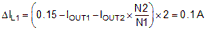
Using the maximum peak-to-peak inductor ripple current ΔIL1 from Equation 21, the minimum inductor value is given by Equation 22.
Equation 22. 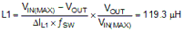
A higher value of 150 µH is selected to ensure the high-side switch current does not exceed the minimum peak current limit threshold.