SNVS480J January   2007  – July 2020 LM5022

PRODUCTION DATA.  

  1. Features
  2. Applications
  3. Description
    1.     Device Images
      1.      Typical Application
  4. Revision History
  5. Pin Configuration and Functions
    1.     Pin Functions
  6. Specifications
    1. 6.1 Absolute Maximum Ratings
    2. 6.2 ESD Ratings
    3. 6.3 Recommended Operating Conditions
    4. 6.4 Thermal Information
    5. 6.5 Electrical Characteristics
    6. 6.6 Typical Characteristics
  7. Detailed Description
    1. 7.1 Overview
    2. 7.2 Functional Block Diagram
    3. 7.3 Feature Description
      1. 7.3.1 High-Voltage Start-Up Regulator
      2. 7.3.2 Input Undervoltage Detector
      3. 7.3.3 Error Amplifier
      4. 7.3.4 Current Sensing and Current Limiting
      5. 7.3.5 PWM Comparator and Slope Compensation
      6. 7.3.6 Soft Start
      7. 7.3.7 MOSFET Gate Driver
      8. 7.3.8 Thermal Shutdown
    4. 7.4 Device Functional Modes
      1. 7.4.1 Oscillator, Shutdown, and SYNC
  8. Application and Implementation
    1. 8.1 Application Information
    2. 8.2 Typical Application
      1. 8.2.1 Design Requirements
      2. 8.2.2 Detailed Design Procedure
        1. 8.2.2.1  Switching Frequency
        2. 8.2.2.2  MOSFET
        3. 8.2.2.3  Output Diode
        4. 8.2.2.4  Boost Inductor
        5. 8.2.2.5  Output Capacitor
        6. 8.2.2.6  VCC Decoupling Capacitor
        7. 8.2.2.7  Input Capacitor
        8. 8.2.2.8  Current Sense Filter
        9. 8.2.2.9  RSNS, RS2, and Current Limit
        10. 8.2.2.10 Control Loop Compensation
        11. 8.2.2.11 Efficiency Calculations
          1. 8.2.2.11.1 Chip Operating Loss
          2. 8.2.2.11.2 MOSFET Switching Loss
          3. 8.2.2.11.3 MOSFET and RSNS Conduction Loss
          4. 8.2.2.11.4 Output Diode Loss
          5. 8.2.2.11.5 Input Capacitor Loss
          6. 8.2.2.11.6 Output Capacitor Loss
          7. 8.2.2.11.7 Boost Inductor Loss
          8. 8.2.2.11.8 Total Loss
          9. 8.2.2.11.9 Efficiency
      3. 8.2.3 Application Curves
  9. Power Supply Recommendations
  10. 10Layout
    1. 10.1 Layout Guidelines
      1. 10.1.1 Filter Capacitors
      2. 10.1.2 Sense Lines
      3. 10.1.3 Compact Layout
      4. 10.1.4 Ground Plane and Shape Routing
    2. 10.2 Layout Examples
  11. 11Device and Documentation Support
    1. 11.1 Device Support
      1. 11.1.1 Third-Party Products Disclaimer
      2. 11.1.2 Development Support
    2. 11.2 Documentation Support
      1. 11.2.1 Related Documentation
    3. 11.3 Receiving Notification of Documentation Updates
    4. 11.4 Support Resources
    5. 11.5 Trademarks
    6. 11.6 Electrostatic Discharge Caution
    7. 11.7 Glossary
  12. 12Mechanical, Packaging, and Orderable Information

Package Options

Mechanical Data (Package|Pins)
Thermal pad, mechanical data (Package|Pins)
Orderable Information

Application Curves

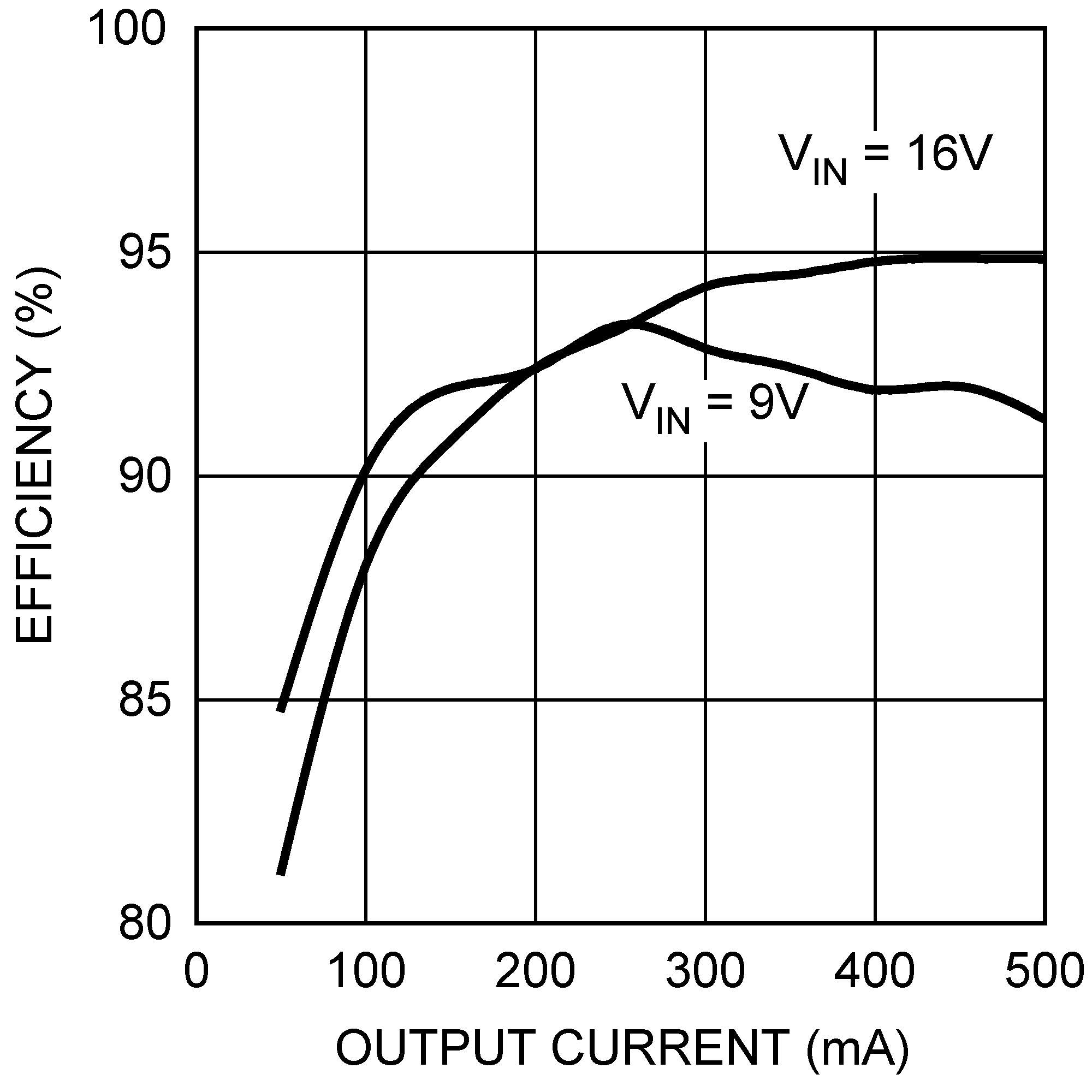
LM5022 Figure 15.png
Figure 22. Efficiency
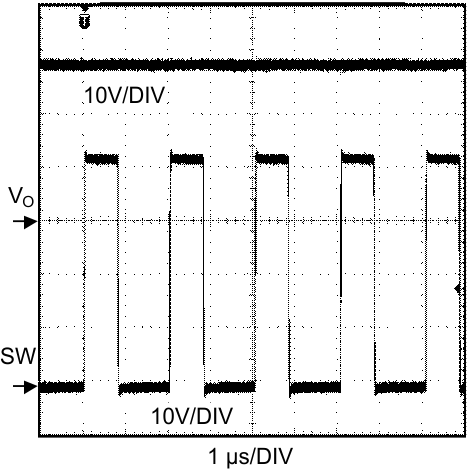
LM5022 Figure_17.gif
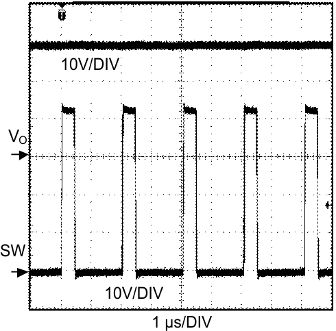
VIN = 16 V, IO = 0.5 A
Figure 24. Switch Node Voltage
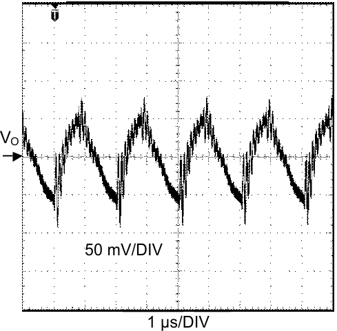
LM5022 Figure_19.gif
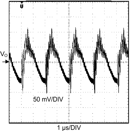
VIN = 16 V, IO = 0.5 A
Figure 26. Output Voltage Ripple AC Coupled
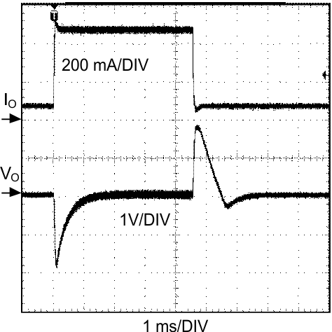
LM5022 Figure_21.gif
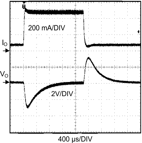
VIN = 16 V, IO = 50 mA to 0.5 A
Figure 28. Load Transient Response
LM5022 Figure_16.gif
VIN = 9 V, IO = 0.5 A
Figure 23. Switch Node Voltage
LM5022 Figure_18.gif
VIN = 9 V, IO = 0.5 A
Figure 25. Output Voltage Ripple AC Coupled
LM5022 Figure_20.gif
VIN = 9 V, IO = 50 mA to 0.5 A
Figure 27. Load Transient Response