SNVS699H February 2011 – January 2015 LM5045
PRODUCTION DATA.
- 1 Features
- 2 Applications
- 3 Description
- 4 Revision History
- 5 Pin Configuration and Functions
- 6 Specifications
-
7 Detailed Description
- 7.1 Overview
- 7.2 Functional Block Diagram
- 7.3
Feature Description
- 7.3.1 High-Voltage Start-Up Regulator
- 7.3.2 Line Undervoltage Detector
- 7.3.3 Overvoltage Protection
- 7.3.4 Reference
- 7.3.5 Oscillator, Sync Input
- 7.3.6 Cycle-by-Cycle Current Limit
- 7.3.7 Hiccup Mode
- 7.3.8 PWM Comparator
- 7.3.9 Ramp Pin
- 7.3.10 Slope Pin
- 7.3.11 Soft-Start
- 7.3.12 Gate Driver Outputs
- 7.3.13 Synchronous Rectifier Control Outputs (SR1 and SR2)
- 7.3.14 Soft-Start of the Synchronous Rectifiers
- 7.3.15 Prebias Startup
- 7.3.16 Soft-Stop
- 7.3.17 Soft-Stop Off
- 7.3.18 Thermal Protection
- 7.4 Device Functional Modes
- 8 Application and Implementation
- 9 Power Supply Recommendations
- 10Layout
- 11Device and Documentation Support
- 12Mechanical, Packaging, and Orderable Information
Package Options
Mechanical Data (Package|Pins)
Thermal pad, mechanical data (Package|Pins)
- PWP|28
Orderable Information
8 Application and Implementation
NOTE
Information in the following applications sections is not part of the TI component specification, and TI does not warrant its accuracy or completeness. TI’s customers are responsible for determining suitability of components for their purposes. Customers should validate and test their design implementation to confirm system functionality.
8.1 Application Information
The LM5045 is a highly integrated PWM controller that contains all of the features necessary for implementing full-bridge topology power converters using either current mode or voltage mode control. The device targets DC-DC converter applications with input voltages of up to 100 Vdc and output power in the range 100 W to 1 kW.
8.2 Typical Application
The following schematic shows an example of a 100W full-bridge converter controlled by LM5045. The operating input voltage range is 36 V to 75 V, and the output voltage is 3.3 V. The output current capability is 30 A. The converter is configured for current mode control with external slope compensation. An auxiliary winding is used to raise the VCC voltage to reduce the controller power dissipation.
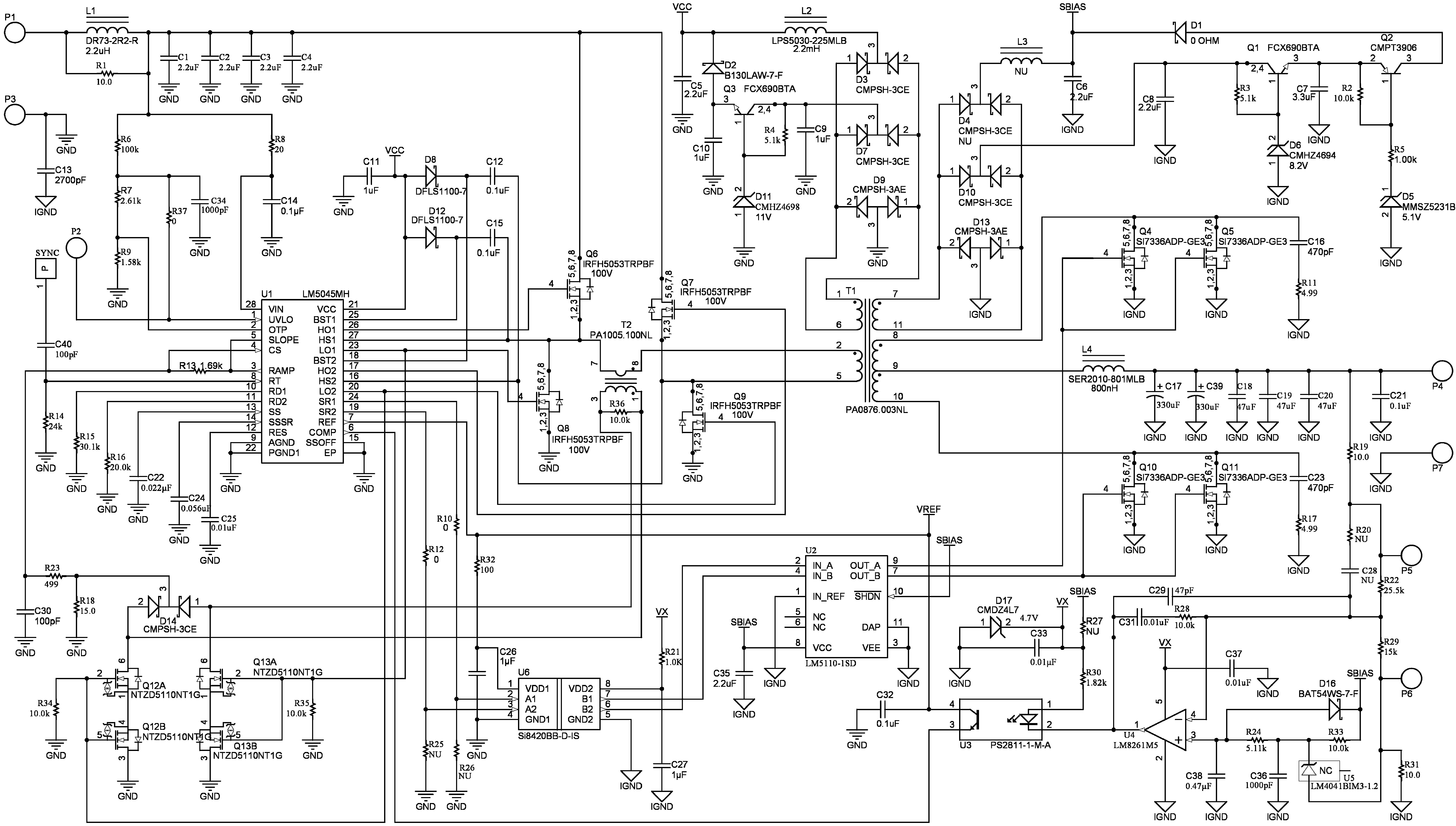 Figure 19. Evaluation Board Schematic
8.2.1 Design Requirements
| PARAMETERS | VALUE |
|---|---|
| Input operating range | 36 V to 75 V |
| Output voltage | 3.3 V |
| Measured efficiency at 48 V | 92% at 30A |
| Frequency of operation | 420 kHz |
| Board size | 2.28 x 1.45 x 0.5 inches |
| Load Regulation | 0.2% |
| Line Regulation | 0.1% |
| Line UVLO | 34V/32V on/off |
| Hiccup Mode | Current Limit |
8.2.2 Detailed Design Procedure
8.2.2.1 VIN and VCC
The voltage applied to the VIN pin, which may be the same as the system voltage applied to the power transformer’s primary (VPWR), can vary in the range of the 14 to 100 V. It is recommended that the filter shown in Figure 20 be used to suppress the transients that may occur at the input supply. This is particularly important when VIN is operated close to the maximum operating rating of the LM5045. The current into VIN depends primarily on the operating current of the LM5045, the switching frequency, and any external loads on the VCC pin, that typically include the gate capacitances of the power MOSFETs. In typical applications, an auxiliary transformer winding is connected through a diode to the VCC pin. This pin must raise VCC voltage above 8 V to shut off the internal start-up regulator.
After the outputs are enabled and the external VCC supply voltage has begun supplying power to the IC, the current into the VIN pin drops below 1mA. VIN should remain at a voltage equal to or above the VCC voltage to avoid reverse current through the internal body diode of the internal VCC regulator.
8.2.2.2 For Applications With > 100 VIN
For applications where the system input voltage exceeds 100 V, VIN can be powered from an external start-up regulator as shown in Figure 21. In this configuration, the VIN and VCC pins should be connected together. The voltage at the VCC and VIN pins must be greater than 10 V (> Max VCC reference voltage) yet not exceed 16 V. To enable operation the VCC voltage must be raised above 10 V. The voltage at the VCC pin must not exceed 16 V. The voltage source at the right side of Figure 21 is typically derived from the power stage, and becomes active once the LM5045’s outputs are active.
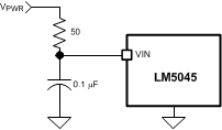 Figure 20. Input Transient Protection
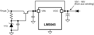 Figure 21. Start-Up Regulator For VPWR > 100 V
8.2.2.3 UVLO and OVP Voltage Divider Selection
Two dedicated comparators connected to the UVLO and OVP pins are used to detect undervoltage and overvoltage conditions. The threshold values of both these comparators are set at 1.25 V. The two functions can be programmed independently with two separate voltage dividers from VIN to AGND as shown in Figure 22 and Figure 23, or with a three-resistor divider as shown in Figure 24. Independent UVLO and OVP pins provide greater flexibility for the user to select the operational voltage range of the system. When the UVLO pin voltage is below 0.4 V, the controller is in a low current shutdown mode. For a UVLO pin voltage greater than 0.4 V but less than 1.25 V the controller is in standby mode. Once the UVLO pin voltage is greater than 1.25 V, the controller is fully enabled. Two external resistors can be used to program the minimum operational voltage for the power converter as shown in Figure 22. When the UVLO pin voltage falls below the 1.25 V threshold, an internal 20 µA current sink is enabled to lower the voltage at the UVLO pin, thus providing threshold hysteresis. Resistance values for R1 and R2 can be determined from the following equations:
where
- VPWR is the desired turnon voltage
- VHYS is the desired UVLO hysteresis at VPWR
For example, if the LM5045 is to be enabled when VPWR reaches 33 V, and disabled when VPWR is decreased to 31 V, R1 should be 100 kΩ, and R2 should be 4.2 kΩ. The voltage at the UVLO pin should not exceed 7 V at any time.
Two external resistors can be used to program the maximum operational voltage for the power converter as shown in Figure 23. When the OVP pin voltage rises above the 1.25 V threshold, an internal 20-µA current source is enabled to raise the voltage at the OVP pin, thus providing threshold hysteresis. Resistance values for R1 and R2 can be determined from the following equations:
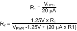
If the LM5045 is to be disabled when VPWR-OFF reaches 80 V and enabled when it is decreased to 78 V. R1 should be 100 kΩ, and R2 should be 1.5 kΩ. The voltage at the OVP pin should not exceed 7 V at any time.
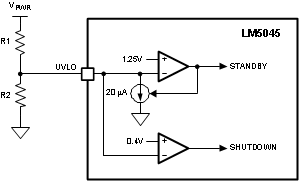 Figure 22. Basic UVLO Configuration
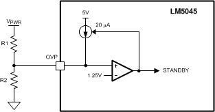 Figure 23. Basic OVP Configuration
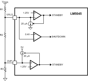 Figure 24. UVLO/OVP Divider
The UVLO and OVP can also be set together using a 3 resistor divider ladder as shown in Figure 24. R1 is calculated as explained in the basic UVLO divider selection. Using the same values, as in the above two examples, for the UVLO and OVP set points, R1 and R3 remain the same at 100 kΩ and 1.5 kΩ. The R2 is 2.7 kΩ obtained by subtracting R3 from 4.2 kΩ.
Remote configuration of the controller’s operational modes can be accomplished with open drain device(s) connected to the UVLO pin as shown in Figure 25.
Figure 26 shows an application of the OVP comparator for Remote Thermal Protection using a thermistor (or multiple thermistors) which may be located near the main heat sources of the power converter. The negative temperature coefficient (NTC) thermistor is nearly logarithmic, and in this example a 100 kΩ thermistor with the β material constant of 4500 Kelvin changes to approximately 2 kΩ at 130ºC. Setting R1 to one-third of this resistance (665 Ω) establishes 130ºC as the desired trip point (for VREF = 5 V). In a temperature band from 20ºC below to 20ºC above the OVP threshold, the voltage divider is nearly linear with 25mV per ºC sensitivity.
R2 provides temperature hysteresis by raising the OVP comparator input by R2 x 20µA. For example, if a 22kΩ resistor is selected for R2, then the OVP pin voltage will increase by 22 kΩ x 20 µA = 506 mV. The NTC temperature must therefore fall by 506 mV / 25 mV per ºC = 20ºC before the LM5045 switches from standby mode to the normal mode.
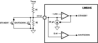 Figure 25. Remote Standby and Disable Control
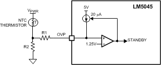 Figure 26. Remote Thermal Protection
8.2.2.4 Current Sense
The CS pin receives an input signal representative of its transformer’s primary current, either from a current sense transformer or from a resistor located at the junction of source pin of the primary switches, as shown in Figure 27 and Figure 28, respectively. In both the cases, the filter components RF and CF should be located as close to the IC as possible, and the ground connection from the current sense transformer, or RSENSE should be a dedicated trace to the appropriate GND pin. Please refer to the Layout section for more layout tips.
The current sense components must provide a signal > 710 mV at the CS pin during an over-load event. Once the voltage on the CS pin crosses the current limit threshold, the current sense comparator terminates the PWM pulse and starts to charge the RES pin. Depending on the configuration of the RES pin, the LM5045 will eventually initiate a hiccup mode restart or be in continuous current limit.
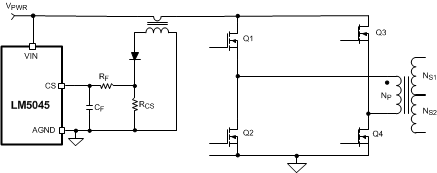 Figure 27. Transformer Current Sense
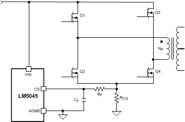 Figure 28. Resistor Current Sense
8.2.2.5 Hiccup Mode Current Limit Restart
The operation of the hiccup mode restart circuit is explained in the section. During a continuous current limit condition, the RES pin is charged with 30 µA current source. The restart delay time required to reach the 1.0 V threshold is given by:

This establishes the time allowed before the IC initiates a hiccup restart sequence. For example, if the CRES = 0.01 µF, the time TCS as noted in Figure 29 below is 334 µs. Once the RES pin reaches 1.0 V, the 30 µA current source is turned-off and a 10 µA current source is turned-on during the ramp up to 4 V and a 5 µA is turned on during the ramp down to 2 V. The hiccup mode off-time is given by:

With a CRES = 0.01 µF, the hiccup time is 49 ms. Once the hiccup time is finished, the RES pin is pulled low and the SS pin is released allowing a soft-start sequence to commence. Once the SS pin reaches 1 V, the PWM pulses will commence. The hiccup mode provides a cool-down period for the power converter in the event of a sustained overload condition thereby lowering the average input current and temperature of the power components during such an event.
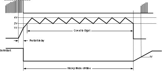 Figure 29. Hiccup Mode Delay and Soft-Start Timing Diagram
8.2.2.6 Augmenting the Gate Drive Strength
The LM5045 includes powerful 2-A integrated gate drivers. However, in certain high-power applications (> 500 W), it might be necessary to augment the strength of the internal gate driver to achieve higher efficiency and better thermal performance. In high power applications, typically, the I2xR loss in the primary MOSFETs is significantly higher than the switching loss. To minimize the I2xR loss, either the primary MOSFETs are paralleled or MOSFETs with low RDS (on) are employed. Both these scenarios increase the total gate charge to be driven by the controller IC. An increase in the gate charge increases the FET transition time and hence increases the switching losses. Therefore, to keep the total losses within a manageable limit the transition time must be reduced.
Generally, during the Miller capacitance charge/discharge the total available driver current is lower during the turnoff process than during the turnon process and often it is enough to speed-up the turnoff time to achieve the efficiency and thermal goals. This can be achieved simply by employing a PNP device, as shown in Figure 30, from gate to source of the power FET. During the turnon process, when the LO1 goes high, the current is sourced through the diode D1 and the BJT Q1 provides the path for the turnoff current. Q1 should be located as close to the power FET as possible so that the turnoff current has the shortest possible path to the ground and does not have to pass through the controller.
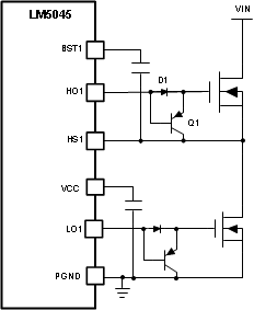 Figure 30. Circuit to Speed-Up the Turnoff Process
Depending on the gate charge characteristics of the primary FET, if it is required to speed up both the turnon and the turnoff time, a bipolar totem pole structure as shown in Figure 31 can be used. When LO1 goes high, the gate to source current is sourced through the NPN transistor Q1 and similar to the circuit shown in Figure 30 when LO1 goes low, the PNP transistor Q2 expedites the turnoff process.
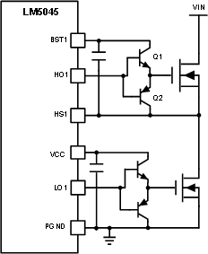 Figure 31. Bipolar Totem Pole Arrangement
Alternatively, a low-side gate driver such as LM5112 can be used instead of the discrete totem pole. The LM5112 comes in a small package with a 3A source and a 7A sink capability. While driving the high-side FET, the HS1 acts as a local ground and the boot capacitor between the BST and HS pins acts as VCC.
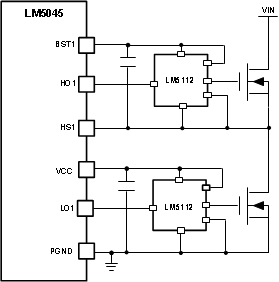 Figure 32. Using a Low-Side Gate Driver to Augment Gate Drive Strength
8.2.3 Application Curve
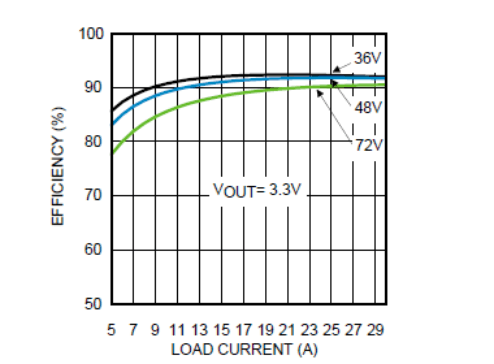 Figure 33. Application Board Efficiency