SNVS629F May   2011  – December 2019 LM5050-1 , LM5050-1-Q1

PRODUCTION DATA.  

  1. Features
  2. Applications
  3. Description
    1.     Device Images
      1.      Full Application
      2.      Typical Redundant Supply Configuration
  4. Revision History
  5. Pin Configuration and Functions
    1.     Pin Functions
  6. Specifications
    1. 6.1 Absolute Maximum Ratings
    2. 6.2 ESD Ratings: LM5050-1
    3. 6.3 ESD Ratings: LM5050-1-Q1
    4. 6.4 Recommended Operating Conditions
    5. 6.5 Thermal Information
    6. 6.6 Electrical Characteristics
    7. 6.7 Typical Characteristics
  7. Detailed Description
    1. 7.1 Overview
    2. 7.2 Functional Block Diagram
    3. 7.3 Feature Description
      1. 7.3.1 IN, GATE, and OUT Pins
      2. 7.3.2 VS Pin
      3. 7.3.3 OFF Pin
    4. 7.4 Device Functional Modes
      1. 7.4.1 ON/OFF Control Mode
      2. 7.4.2 External Power Supply Mode
  8. Application and Implementation
    1. 8.1 Application Information
      1. 8.1.1 MOSFET Selection
      2. 8.1.2 Short Circuit Failure of an Input Supply
    2. 8.2 Typical Applications
      1. 8.2.1 Typical Application With Input and Output Transient Protection
        1. 8.2.1.1 Design Requirements
        2. 8.2.1.2 Detailed Design Procedure
          1. 8.2.1.2.1 Power Supply Components (R1 C1,) Selection
          2. 8.2.1.2.2 MOSFET (Q1) Selection
          3. 8.2.1.2.3 D1 and D2 Selection for Inductive Kick-Back Protection
        3. 8.2.1.3 Application Curves
      2. 8.2.2 Using a Separate VS Supply for Low Vin Operation
      3. 8.2.3 ORing of Two Power Sources
      4. 8.2.4 Reverse Input Voltage Protection With IQ Reduction
      5. 8.2.5 Basic Application With Input Transient Protection
      6. 8.2.6 48-V Application With Reverse Input Voltage (VIN = –48 V) Protection
        1. 8.2.6.1 Application Curves
  9. Power Supply Recommendations
  10. 10Layout
    1. 10.1 Layout Guidelines
    2. 10.2 Layout Example
  11. 11Device and Documentation Support
    1. 11.1 Documentation Support
      1. 11.1.1 Related Documentation
    2. 11.2 Related Links
    3. 11.3 Community Resources
    4. 11.4 Trademarks
    5. 11.5 Electrostatic Discharge Caution
    6. 11.6 Glossary
  12. 12Mechanical, Packaging, and Orderable Information

Package Options

Mechanical Data (Package|Pins)
Thermal pad, mechanical data (Package|Pins)
Orderable Information

Typical Characteristics

Unless otherwise stated: VVS = 12 V, VIN = 12 V, VOFF = 0 V, and TJ = 25°C
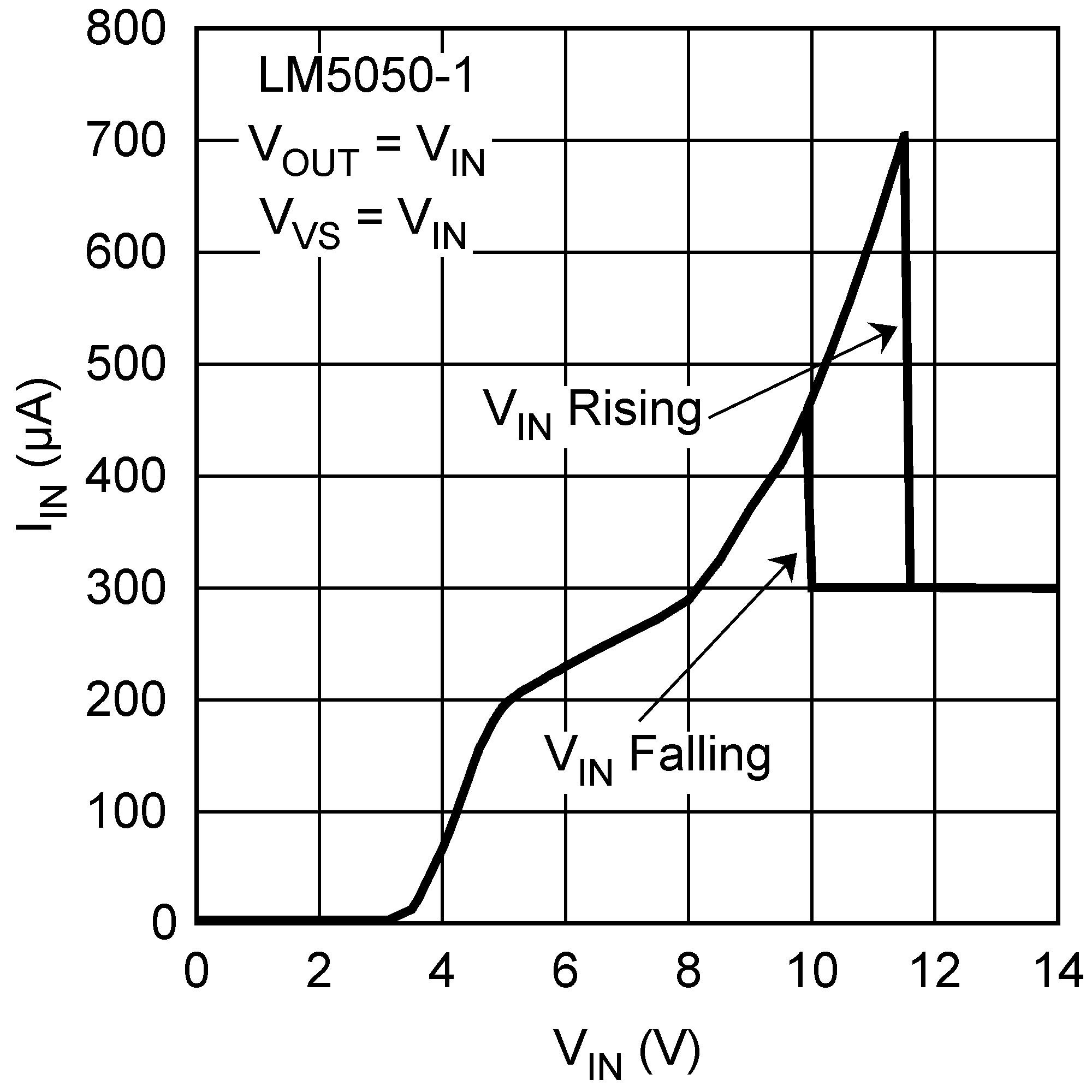
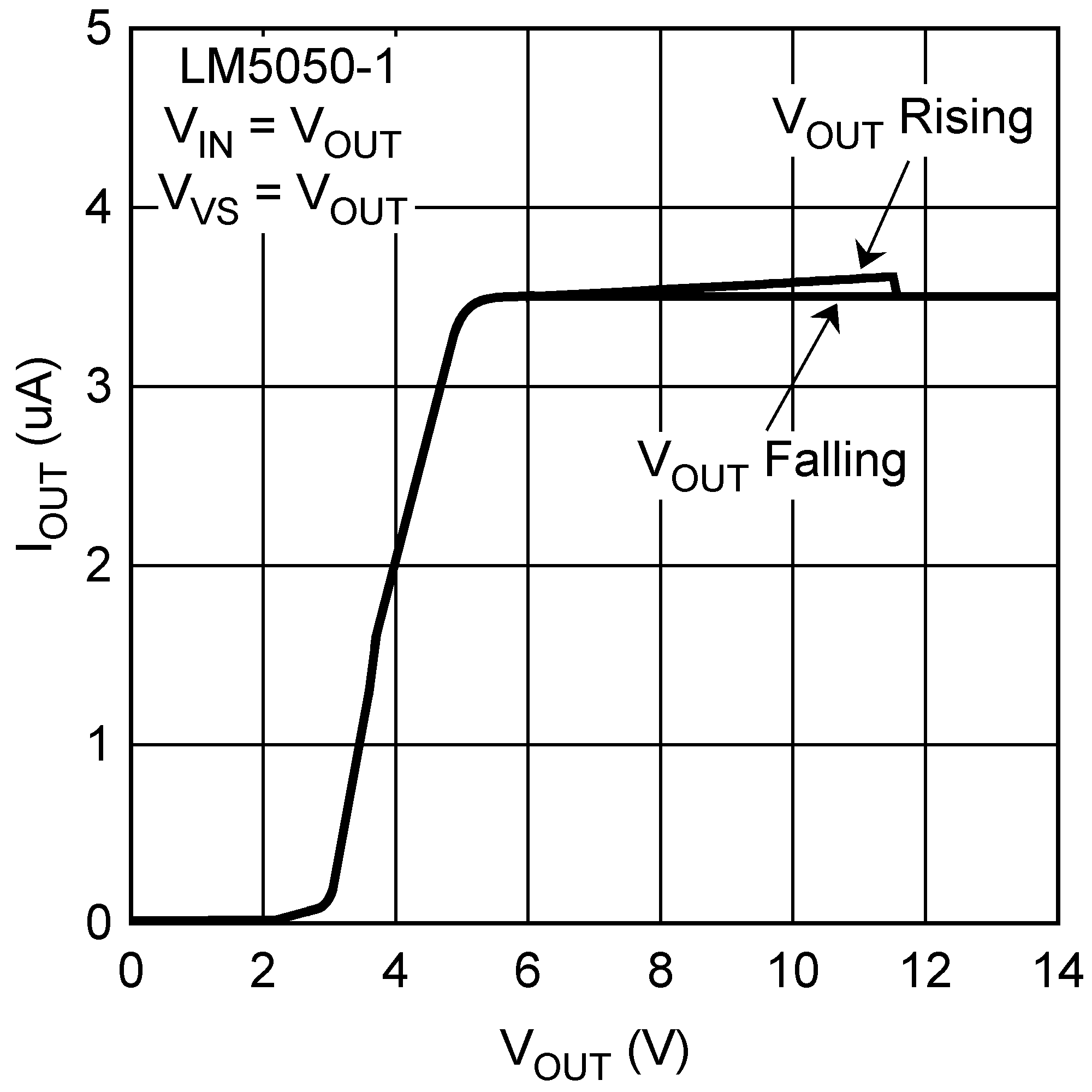
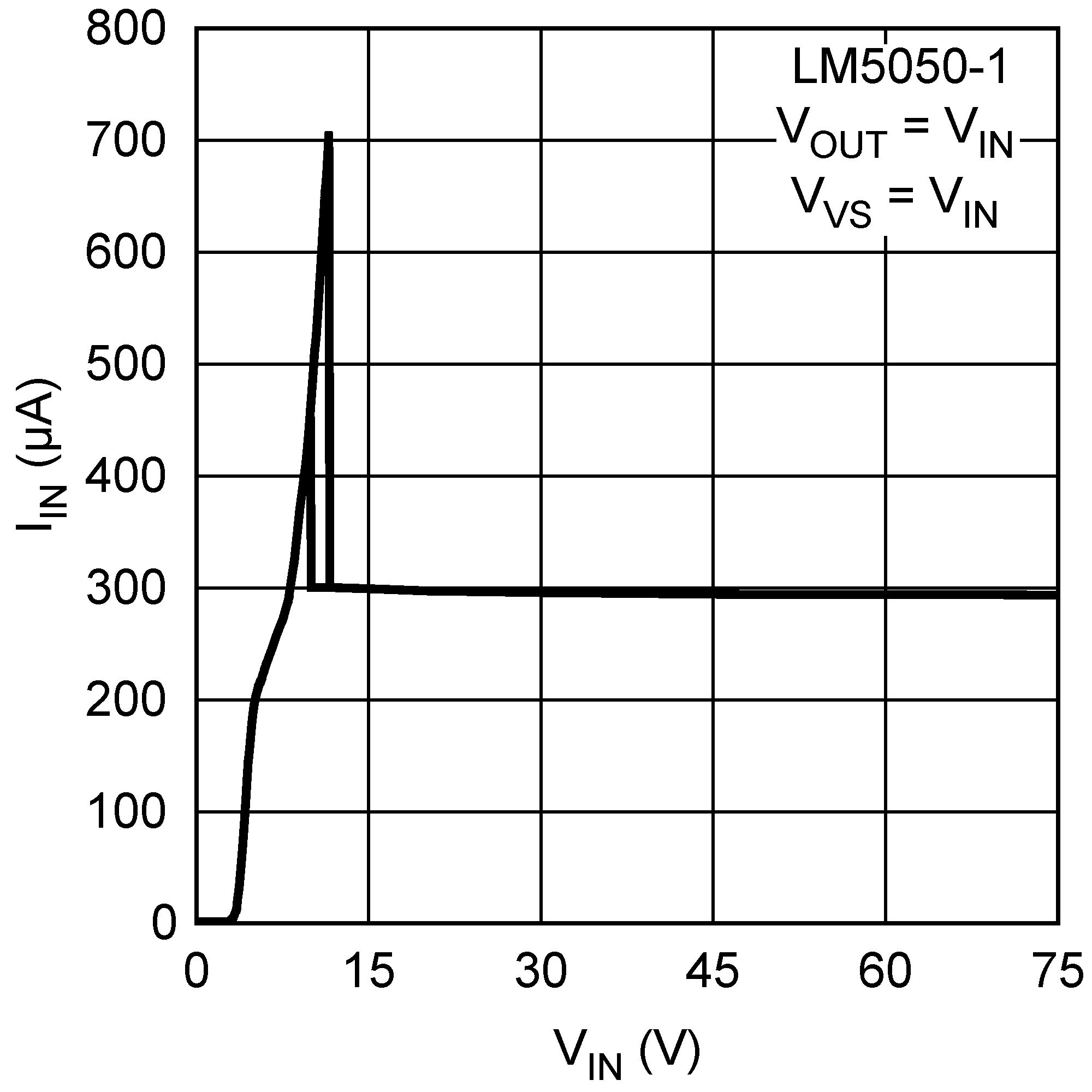
LM5050-1 LM5050-1-Q1 30104834.png
Figure 3. IIN vs VIN
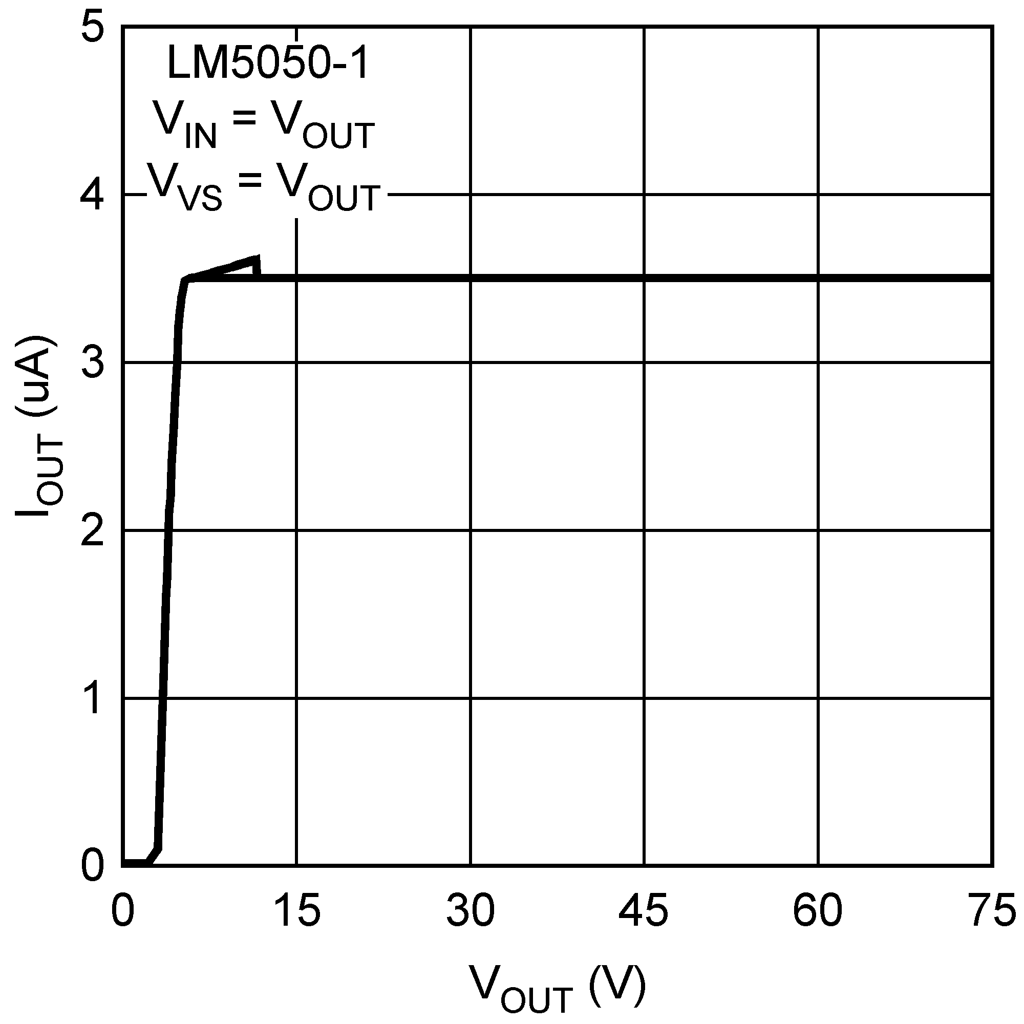
LM5050-1 LM5050-1-Q1 30104835.png
Figure 5. IOUT vs VOUT
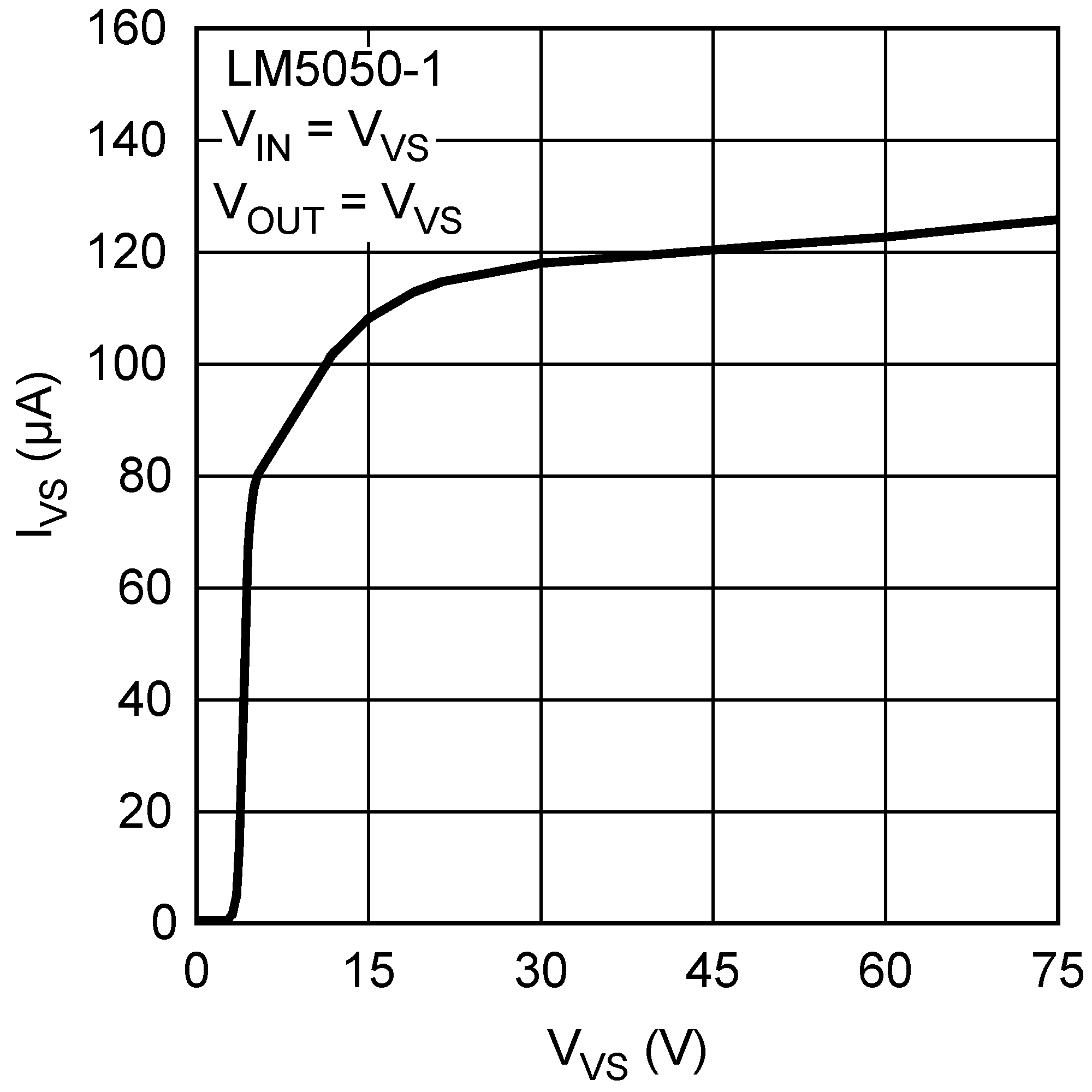
LM5050-1 LM5050-1-Q1 30104836.png
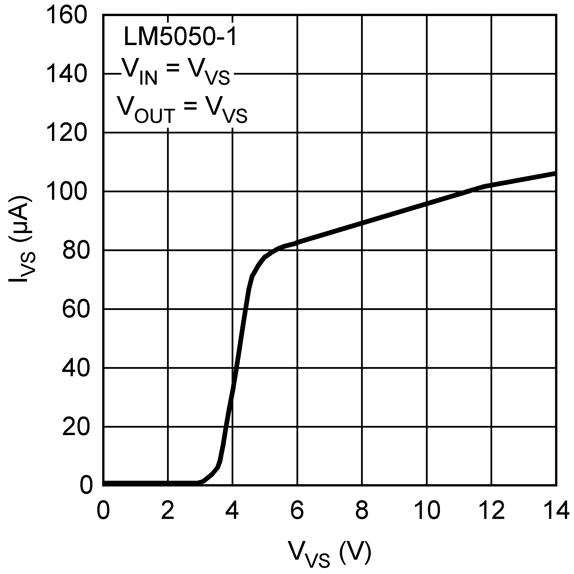
Figure 7. IVS vs VVS
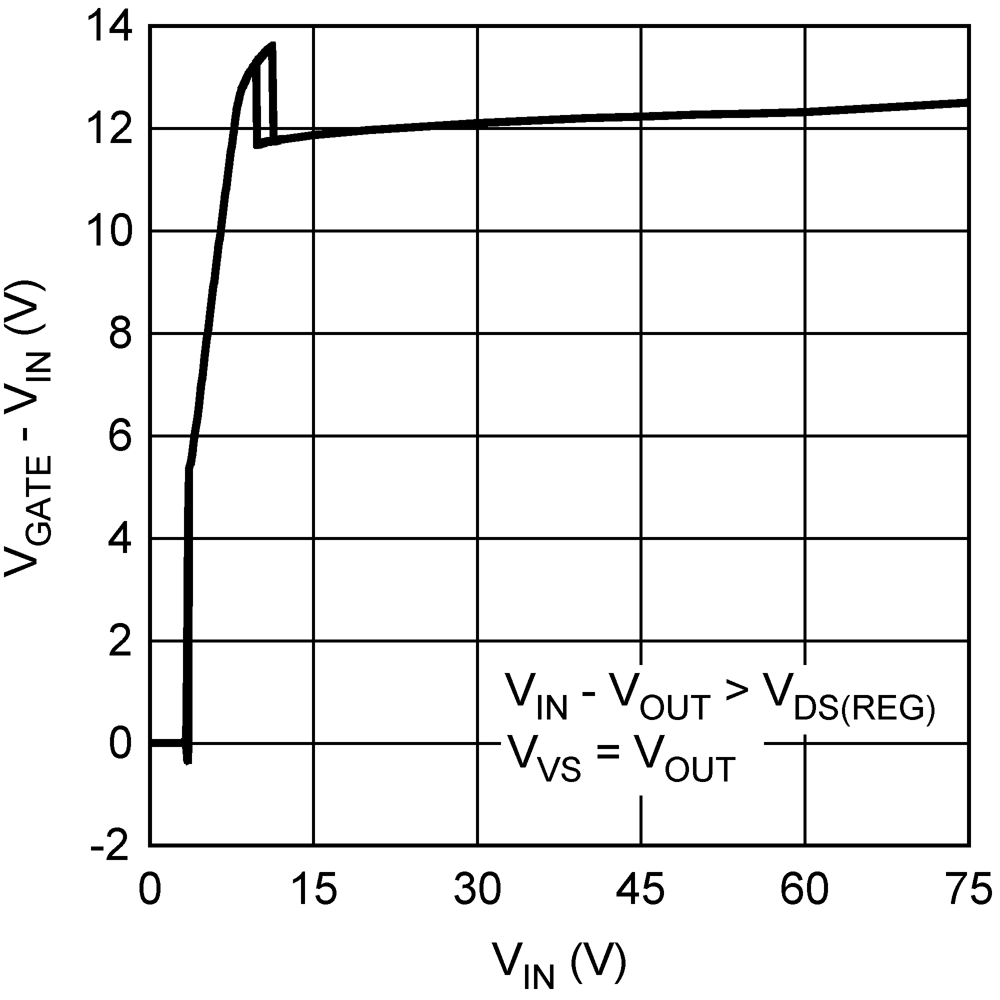
LM5050-1 LM5050-1-Q1 30104811.png
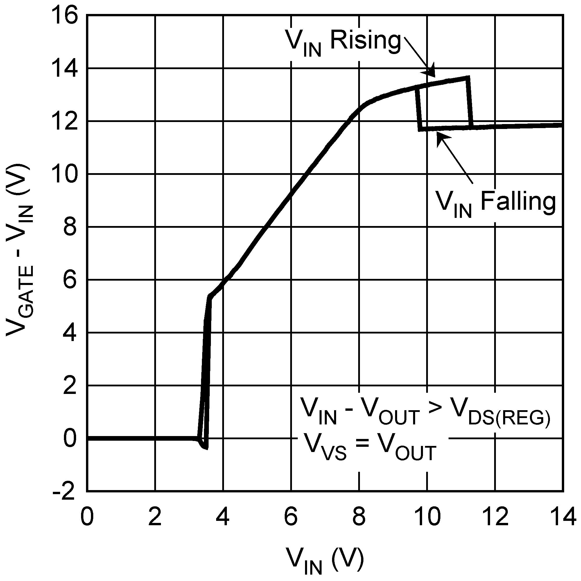
Figure 9. (VGATE - VIN) vs VIN, VVS = VOUT
LM5050-1 LM5050-1-Q1 30104847.gif
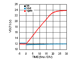
Figure 11. Forward CGATE Charge Time, CGATE = 47 nF
LM5050-1 LM5050-1-Q1 30104829.png
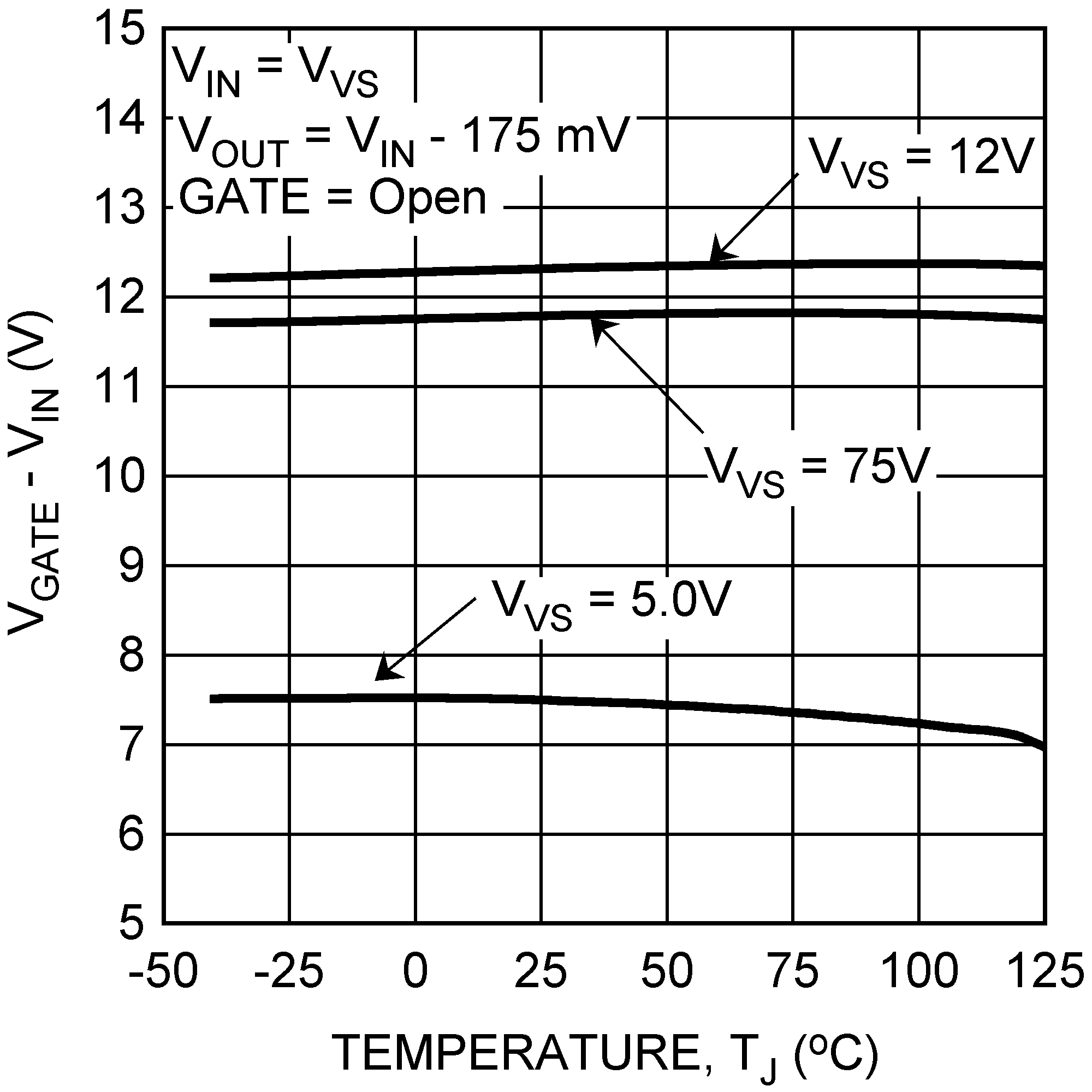
Figure 13. VGATE - VIN vs Temperature
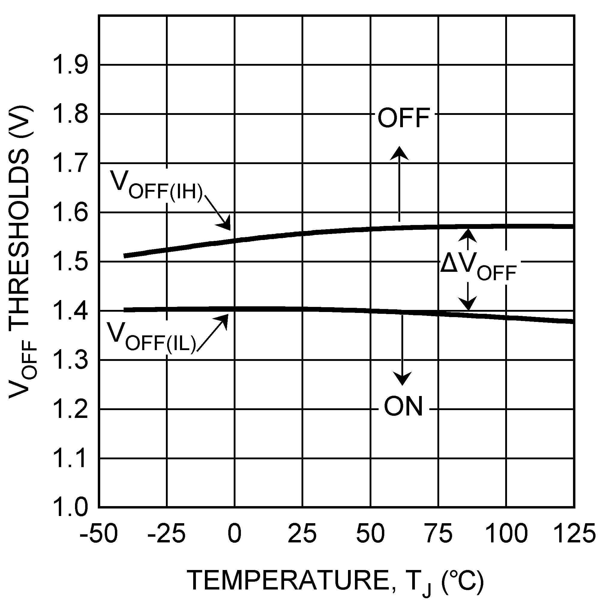
LM5050-1 LM5050-1-Q1 30104827.png
Figure 15. OFF Pin Thresholds vs Temperature
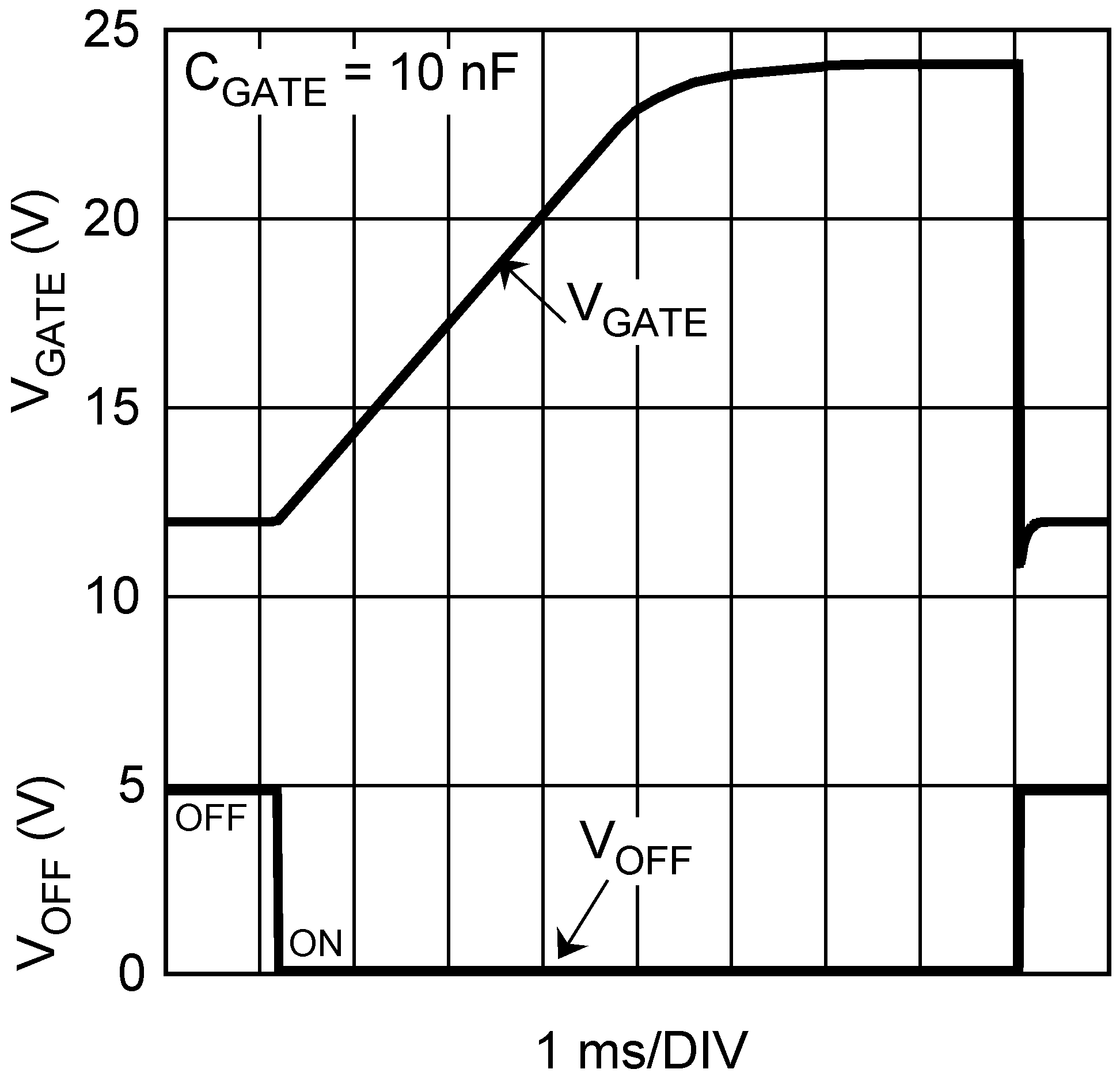
LM5050-1 LM5050-1-Q1 30104815.png
Figure 17. CGATE Charge and Discharge vs OFF Pin
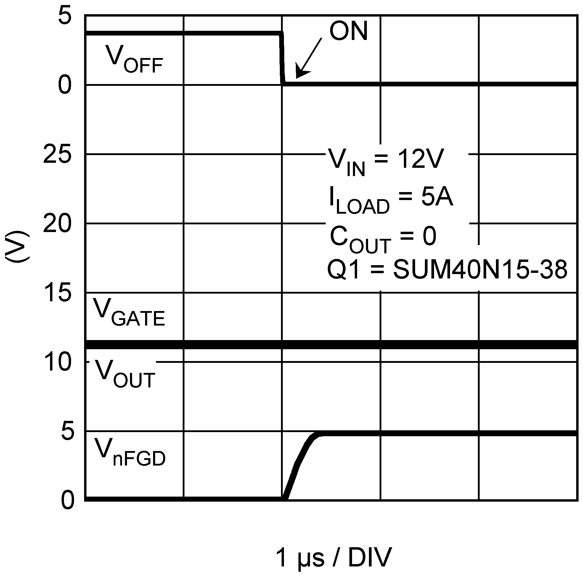
LM5050-1 LM5050-1-Q1 30104817.png
Figure 19. OFF Pin, OFF to ON Transition
LM5050-1 LM5050-1-Q1 30104819.png
Figure 4. IIN vs VIN
LM5050-1 LM5050-1-Q1 30104820.png
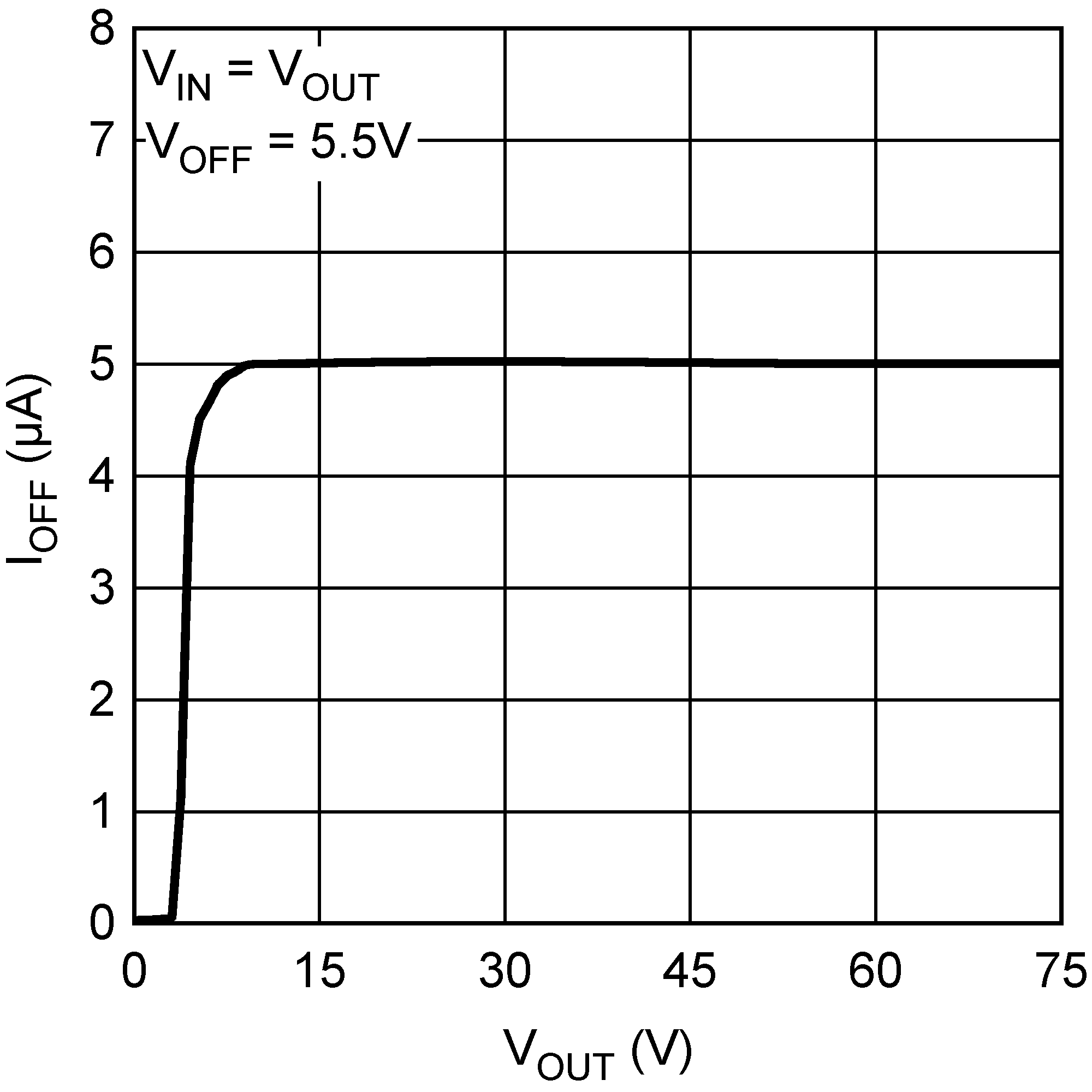
Figure 6. IOUT vs VOUT
LM5050-1 LM5050-1-Q1 30104821.png
Figure 8. IVS vs VVS
LM5050-1 LM5050-1-Q1 30104812.png
Figure 10. (VGATE - VIN) vs VIN, VVS = VOUT
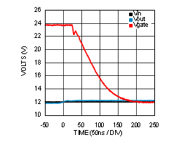
LM5050-1 LM5050-1-Q1 30104846.gif
Figure 12. Reverse CGATE Discharge, CGATE = 47 nF
LM5050-1 LM5050-1-Q1 30104830.png
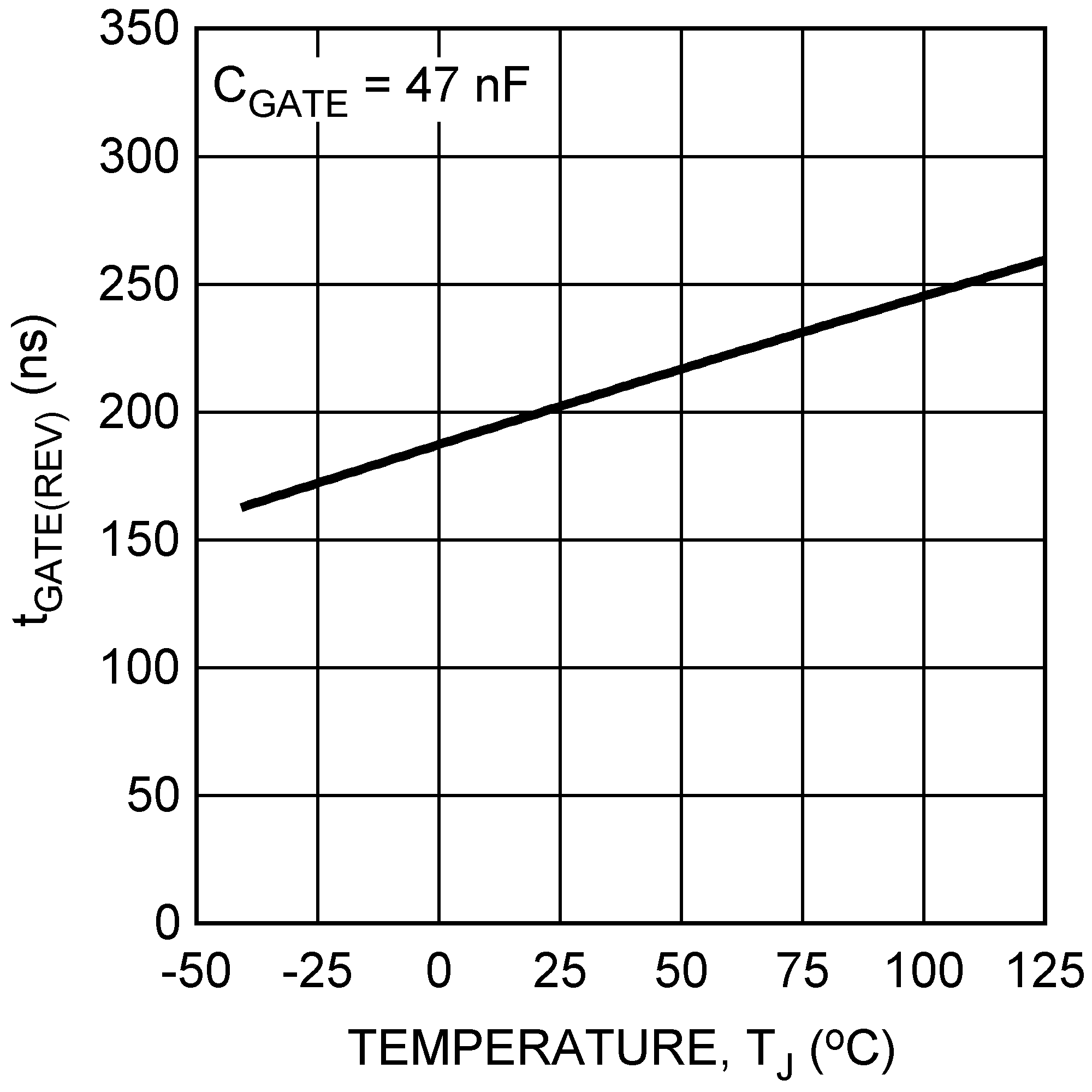
Figure 14. tGATE(REV) vs Temperature
LM5050-1 LM5050-1-Q1 30104828.png
Figure 16. OFF Pin Pulldown vs Temperature
LM5050-1 LM5050-1-Q1 30104816.png
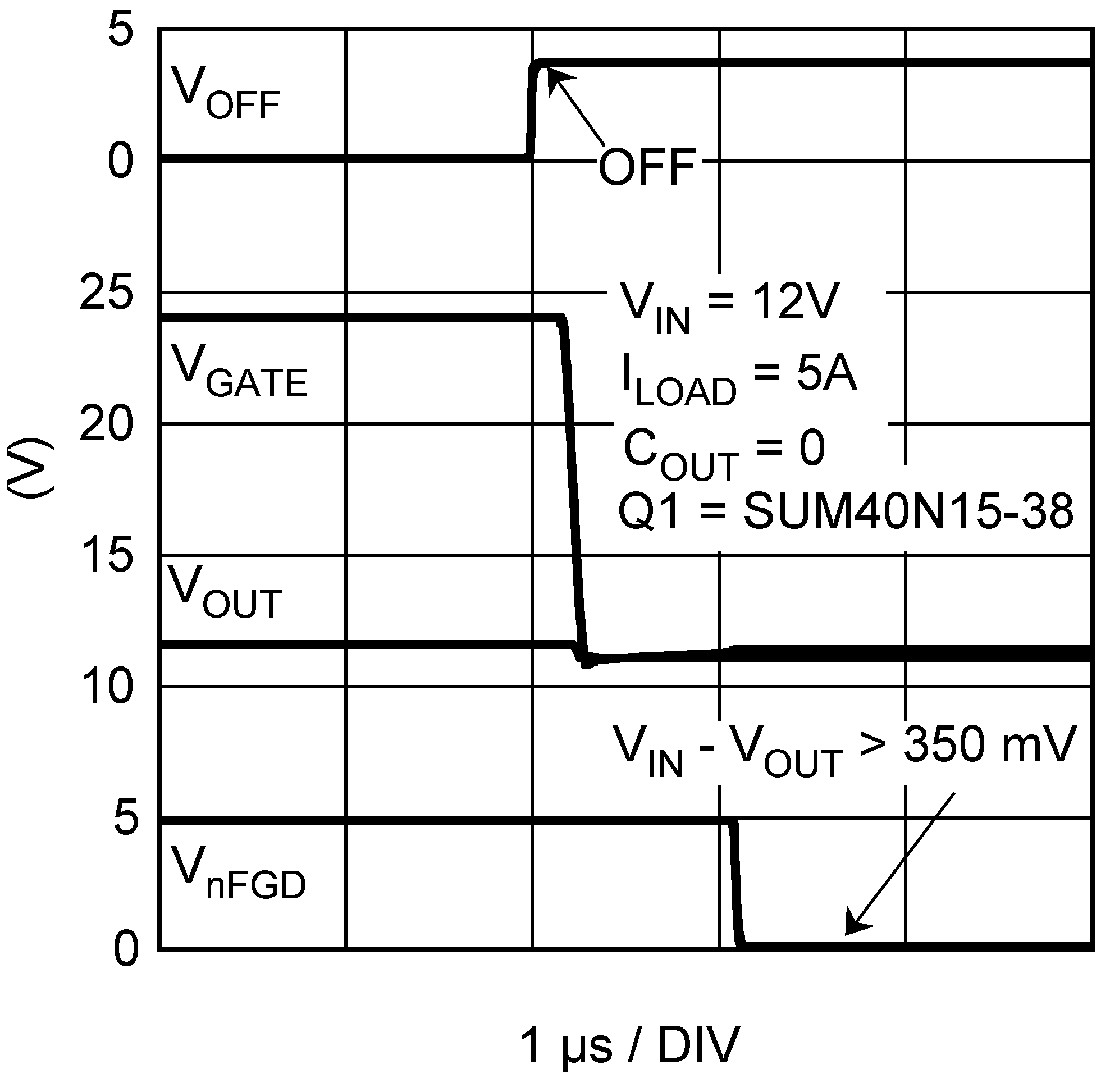
Figure 18. OFF Pin, ON to OFF Transition
LM5050-1 LM5050-1-Q1 30104818.png
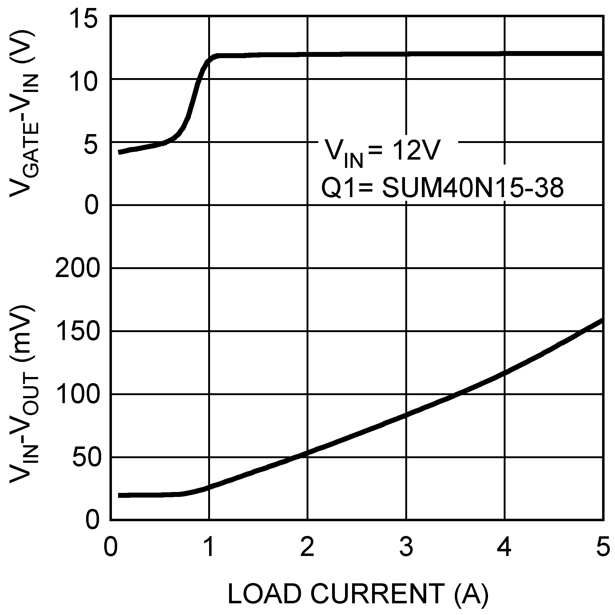
Figure 20. GATE Pin vs (RDS(ON) × IDS)