SNVS600J December 2008 – June 2022 LM5088 , LM5088-Q1
PRODUCTION DATA
- 1 Features
- 2 Applications
- 3 Description
- 4 Revision History
- 5 Pin Configuration and Functions
- 6 Specifications
-
7 Detailed Description
- 7.1 Overview
- 7.2 Functional Block Diagram
- 7.3
Feature Description
- 7.3.1 High Voltage Low-Dropout Regulator
- 7.3.2 Line Undervoltage Detector
- 7.3.3 Oscillator and Sync Capability
- 7.3.4 Error Amplifier and PWM Comparator
- 7.3.5 Ramp Generator
- 7.3.6 Dropout Voltage Reduction
- 7.3.7 Frequency Dithering (LM5088-1 Only)
- 7.3.8 Cycle-by-Cycle Current Limit
- 7.3.9 Overload Protection Timer (LM5088-2 Only)
- 7.3.10 Soft Start
- 7.3.11 HG Output
- 7.3.12 Thermal Protection
- 7.4 Device Functional Modes
-
8 Application and Implementation
- 8.1 Application Information
- 8.2
Typical Application
- 8.2.1 Design Requirements
- 8.2.2
Detailed Design Procedure
- 8.2.2.1 Timing Resistor
- 8.2.2.2 Output Inductor
- 8.2.2.3 Current Sense Resistor
- 8.2.2.4 Ramp Capacitor
- 8.2.2.5 Output Capacitors
- 8.2.2.6 Input Capacitors
- 8.2.2.7 VCC Capacitor
- 8.2.2.8 Bootstrap Capacitor
- 8.2.2.9 Soft-Start Capacitor
- 8.2.2.10 Output Voltage Divider
- 8.2.2.11 UVLO Divider
- 8.2.2.12 Restart Capacitor (LM5008-2 Only)
- 8.2.2.13 MOSFET Selection
- 8.2.2.14 Diode Selection
- 8.2.2.15 Snubber Components Selection
- 8.2.2.16 Error Amplifier Compensation
- 8.2.3 Application Curves
- 9 Power Supply Recommendations
- 10Layout
- 11Device and Documentation Support
- 12Mechanical, Packaging, and Orderable Information
Package Options
Mechanical Data (Package|Pins)
- PWP|16
Thermal pad, mechanical data (Package|Pins)
- PWP|16
Orderable Information
7.3.6 Dropout Voltage Reduction
The LM5088 features unique circuitry to reduce the dropout voltage. Dropout voltage is defined as the difference between the minimum input voltage to maintain regulation and the output voltage (VIN(min) – VOUT). Dropout voltage thus determines the lowest input voltage at which the converter maintains regulation. In a buck converter, dropout voltage primarily depends upon the maximum duty cycle. The maximum duty cycle is dependent on the oscillator frequency and minimum off time.
An approximation for the dropout voltage is:
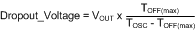
where
- TOSC = 1 / fSW.
- TOFF (max) is the forced off time (280 ns typical, 365 ns maximum).
- fSW is the oscillator frequency.
- TOSC is the oscillator period.
From the above equation, it can be seen that for a given output voltage, reducing the dropout voltage requires either reducing the forced off time or oscillator frequency (1/TOSC). The forced off time is limited by the time required to replenish the bootstrap capacitor and time required to sample the re-circulating diode current. The 365-ns forced off time of the LM5088 controller is a good trade-off between these two requirements. Thus, the LM5088 reduces dropout voltage by dynamically decreasing the operating frequency during dropout. The dynamic frequency control (DFC) is achieved using a dropout monitor, which detects a dropout condition and reduces the operating frequency. The operating frequency continues to decrease with decreasing input voltage until the frequency falls to the minimum value set by the DFC circuitry.
If the VIN voltage continues to fall below this point, output regulation can no longer be maintained. The oscillator frequency reverts back to the nominal operating frequency set by the RT resistor when the input voltage increases above the dropout range. DFC circuitry does not affect the PWM during normal operating conditions.
 Figure 7-4 Dropout Voltage Reduction using Dynamic Frequency Control