SNVS499I February 2007 – November 2023 LM5116
PRODUCTION DATA
- 1
- 1 Features
- 2 Applications
- 3 Description
- 4 Pin Configuration and Functions
- 5 Specifications
- 6 Detailed Description
-
7 Application and Implementation
- 7.1 Application Information
- 7.2
Typical Application
- 7.2.1 Design Requirements
- 7.2.2
Detailed Design Procedure
- 7.2.2.1 Custom Design with WEBENCH® Tools
- 7.2.2.2 Timing Resistor
- 7.2.2.3 Output Inductor
- 7.2.2.4 Current Sense Resistor
- 7.2.2.5 Ramp Capacitor
- 7.2.2.6 Output Capacitors
- 7.2.2.7 Input Capacitors
- 7.2.2.8 VCC Capacitor
- 7.2.2.9 Bootstrap Capacitor
- 7.2.2.10 Soft Start Capacitor
- 7.2.2.11 Output Voltage Divider
- 7.2.2.12 UVLO Divider
- 7.2.2.13 MOSFETs
- 7.2.2.14 MOSFET Snubber
- 7.2.2.15 Error Amplifier Compensation
- 7.2.2.16 Comprehensive Equations
- 7.2.3 Application Curves
- 7.3 Power Supply Recommendations
- 7.4 Layout
- 8 Device and Documentation Support
- 9 Revision History
- 10Mechanical, Packaging, and Orderable Information
Package Options
Mechanical Data (Package|Pins)
- PWP|20
Thermal pad, mechanical data (Package|Pins)
- PWP|20
Orderable Information
7.2.2.15 Error Amplifier Compensation
RCOMP, CCOMP and CHF configure the error amplifier gain characteristics to accomplish a stable voltage loop gain. One advantage of current mode control is the ability to close the loop with only two feedback components, RCOMP and CCOMP. The voltage loop gain is the product of the modulator gain and the error amplifier gain. For the 5-V output design example, the modulator is treated as an ideal voltage-to-current converter. The DC modulator gain of the LM5116 can be modeled as:
The dominant low frequency pole of the modulator is determined by the load resistance (RLOAD) and output capacitance (COUT). The corner frequency of this pole is:
For RLOAD = 5 V / 7 A = 0.714 Ω and COUT = 320 µF (effective) then fP(MOD) = 700 Hz
DC Gain(MOD) = 0.714 Ω / (10 ✕ 10 mΩ) = 7.14 = 17 dB
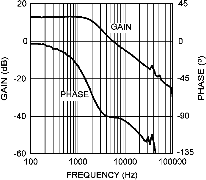
For the 5-V design example the modulator gain vs. frequency characteristic was measured as shown in Figure 7-3.
 Figure 7-3 Modulator Gain and Phase
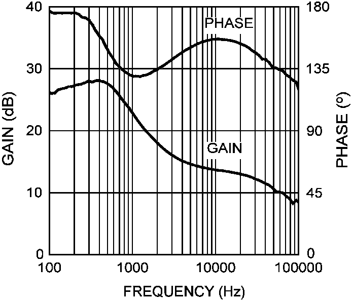
Components RCOMP and CCOMP configure the error amplifier as a type II configuration. The DC gain of the amplifier is 80 dB which has a pole at low frequency and a zero at fZEA = 1 / (2π ✕ RCOMP ✕ CCOMP). The error amplifier zero cancels the modulator pole leaving a single pole response at the crossover frequency of the voltage loop. A single pole response at the crossover frequency yields a very stable loop with 90° of phase margin. For the design example, a target loop bandwidth (crossover frequency) of one-tenth the switching frequency or 25 kHz was selected. The compensation network zero (fZEA) must be selected at least an order of magnitude less than the target crossover frequency. This constrains the product of RCOMP and CCOMP for a desired compensation network zero 1 / (2π ✕ RCOMP ✕ CCOMP) to be 2.5 kHz. Increasing RCOMP, while proportionally decreasing CCOMP, increases the error amp gain. Conversely, decreasing RCOMP while proportionally increasing CCOMP, decreases the error amp gain. For the design example CCOMP was selected as 3300 pF and RCOMP was selected as 18 kΩ. These values configure the compensation network zero at 2.7 kHz. The error amp gain at frequencies greater than fZEA is: RCOMP / RFB2, which is approximately 4.8 (13.6 dB).
 Figure 7-4 Error Amplifier Gain and Phase
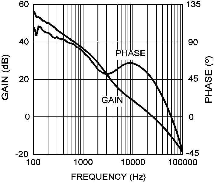
The overall voltage loop gain can be predicted as the sum (in dB) of the modulator gain and the error amp gain.
 Figure 7-5 Overall Voltage Loop Gain and Phase
If a network analyzer is available, the modulator gain can be measured and the error amplifier gain can be configured for the desired loop transfer function. If a network analyzer is not available, the error amplifier compensation components can be designed with the guidelines given. Step load transient tests can be performed to verify acceptable performance. The step load goal is minimum overshoot with a damped response. CHF can be added to the compensation network to decrease noise susceptibility of the error amplifier. The value of CHF must be sufficiently small because the addition of this capacitor adds a pole in the error amplifier transfer function. This pole must be well beyond the loop crossover frequency. A good approximation of the location of the pole added by CHF is: fP2 = fZEA ✕ CCOMP / CHF. The value of CHF was selected as 100 pF for the design example.