SNVSBC2A June 2019 – April 2024 LM5163-Q1
PRODUCTION DATA
- 1
- 1 Features
- 2 Applications
- 3 Description
- 4 Pin Configuration and Functions
- 5 Specifications
-
6 Detailed Description
- 6.1 Overview
- 6.2 Functional Block Diagram
- 6.3
Feature Description
- 6.3.1 Control Architecture
- 6.3.2 Internal VCC Regulator and Bootstrap Capacitor
- 6.3.3 Regulation Comparator
- 6.3.4 Internal Soft Start
- 6.3.5 On-Time Generator
- 6.3.6 Current Limit
- 6.3.7 N-Channel Buck Switch and Driver
- 6.3.8 Synchronous Rectifier
- 6.3.9 Enable/Undervoltage Lockout (EN/UVLO)
- 6.3.10 Power Good (PGOOD)
- 6.3.11 Thermal Protection
- 6.4 Device Functional Modes
- 7 Application and Implementation
- 8 Device and Documentation Support
- 9 Revision History
- 10Mechanical, Packaging, and Orderable Information
Package Options
Mechanical Data (Package|Pins)
- DDA|8
Thermal pad, mechanical data (Package|Pins)
- DDA|8
Orderable Information
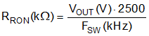
7.2.2.2 Switching Frequency (RRON)
The switching frequency of the LM5163-Q1 is set by the on-time programming resistor placed at RON. As shown by Equation 15, a standard 100-kΩ, 1% resistor sets the switching frequency at 300 kHz.
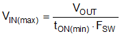
Note that at very low duty cycles, the 50 ns minimum controllable on-time of the high-side MOSFET, tON(min), limits the maximum switching frequency. In CCM, tON(min) limits the voltage conversion step-down ratio for a given switching frequency. Use Equation 16 to calculate the minimum controllable duty cycle.

Ultimately, the choice of switching frequency for a given output voltage affects the available input voltage range, solution size, and efficiency. Use Equation 17 to calculate the maximum supply voltage for a given tON(min) before switching frequency reduction occurs.