SNVSAU4C September 2018 – April 2024 LM5164
PRODUCTION DATA
- 1
- 1 Features
- 2 Applications
- 3 Description
- 4 Pin Configuration and Functions
- 5 Specifications
-
6 Detailed Description
- 6.1 Overview
- 6.2 Functional Block Diagram
- 6.3
Feature Description
- 6.3.1 Control Architecture
- 6.3.2 Internal VCC Regulator and Bootstrap Capacitor
- 6.3.3 Regulation Comparator
- 6.3.4 Internal Soft Start
- 6.3.5 On-Time Generator
- 6.3.6 Current Limit
- 6.3.7 N-Channel Buck Switch and Driver
- 6.3.8 Synchronous Rectifier
- 6.3.9 Enable/Undervoltage Lockout (EN/UVLO)
- 6.3.10 Power Good (PGOOD)
- 6.3.11 Thermal Protection
- 6.4 Device Functional Modes
- 7 Application and Implementation
- 8 Device and Documentation Support
- 9 Revision History
- 10Mechanical, Packaging, and Orderable Information
Package Options
Refer to the PDF data sheet for device specific package drawings
Mechanical Data (Package|Pins)
- DDA|8
Thermal pad, mechanical data (Package|Pins)
Orderable Information
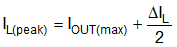
7.2.2.3 Buck Inductor (LO)
Use Equation 18 and Equation 19 to calculate the inductor ripple current (assuming CCM operation) and peak inductor current, respectively.
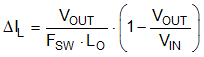
For most applications, choose an inductance such that the inductor ripple current, ΔIL, is between 30% and 50% of the rated load current at nominal input voltage. Use Equation 20 to calculate the inductance.
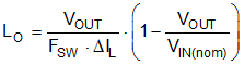
Choosing a 68-μH inductor in this design results in 447-mA peak-to-peak ripple current at a nominal input voltage of 48 V, equivalent to 45% of the 1-A rated load current.
Check the inductor data sheet to make sure the saturation current of the inductor is well above the current limit setting of the LM5164. Ferrite-core inductors have relatively lower core losses and are preferred at high switching frequencies, but exhibit a hard saturation characteristic – the inductance collapses abruptly when the saturation current is exceeded. This results in an abrupt increase in inductor ripple current, higher output voltage ripple, and reduced efficiency, in turn compromising reliability. Note that inductor saturation current levels generally decrease as the core temperature increases.