SNVSAJ3C March   2016  – December 2022 LM5165-Q1

PRODUCTION DATA  

  1. Features
  2. Applications
  3. Description
  4. Revision History
  5. Pin Configuration and Functions
  6. Specifications
    1. 6.1 Absolute Maximum Ratings
    2. 6.2 ESD Ratings
    3. 6.3 Recommended Operating Conditions
    4. 6.4 Thermal Information
    5. 6.5 Electrical Characteristics
    6. 6.6 Switching Characteristics
    7. 6.7 Typical Characteristics
  7. Detailed Description
    1. 7.1 Overview
    2. 7.2 Functional Block Diagram
    3. 7.3 Feature Description
      1. 7.3.1  Integrated Power MOSFETs
      2. 7.3.2  Selectable PFM or COT Mode Converter Operation
      3. 7.3.3  COT Mode Light-Load Operation
      4. 7.3.4  Low Dropout Operation and 100% Duty Cycle Mode
      5. 7.3.5  Adjustable Output Voltage (FB)
      6. 7.3.6  Adjustable Current Limit
      7. 7.3.7  Precision Enable (EN) and Hysteresis (HYS)
      8. 7.3.8  Power Good (PGOOD)
      9. 7.3.9  Configurable Soft Start (SS)
      10. 7.3.10 Thermal Shutdown
    4. 7.4 Device Functional Modes
      1. 7.4.1 Shutdown Mode
      2. 7.4.2 Standby Mode
      3. 7.4.3 Active Mode in COT
      4. 7.4.4 Active Mode in PFM
      5. 7.4.5 Sleep Mode in PFM
  8. Applications and Implementation
    1. 8.1 Application Information
    2. 8.2 Typical Applications
      1. 8.2.1 Design 1: Wide VIN, Low IQ COT Converter Rated at 5 V, 150 mA
        1. 8.2.1.1 Design Requirements
        2. 8.2.1.2 Detailed Design Procedure
          1. 8.2.1.2.1 Custom Design With WEBENCH® Tools
          2. 8.2.1.2.2 Switching Frequency – RT
          3. 8.2.1.2.3 Filter Inductor – LF
          4. 8.2.1.2.4 Output Capacitors – COUT
          5. 8.2.1.2.5 Series Ripple Resistor – RESR
          6. 8.2.1.2.6 Input Capacitor – CIN
          7. 8.2.1.2.7 Soft-Start Capacitor – CSS
        3. 8.2.1.3 Application Curves
      2. 8.2.2 Design 2: Small Solution Size PFM Converter Rated at 3.3 V, 50 mA
        1. 8.2.2.1 Design Requirements
        2. 8.2.2.2 Detailed Design Procedure
          1. 8.2.2.2.1 Peak Current Limit Setting – RILIM
          2. 8.2.2.2.2 Switching Frequency – LF
          3. 8.2.2.2.3 Output Capacitor – COUT
          4. 8.2.2.2.4 Input Capacitor – CIN
        3. 8.2.2.3 Application Curves
      3. 8.2.3 Design 3: High Density 12-V, 75-mA PFM Converter
        1. 8.2.3.1 Design Requirements
        2. 8.2.3.2 Detailed Design Procedure
          1. 8.2.3.2.1 Peak Current Limit Setting – RILIM
          2. 8.2.3.2.2 Switching Frequency – LF
          3. 8.2.3.2.3 Input and Output Capacitors – CIN, COUT
          4. 8.2.3.2.4 Feedback Resistors – RFB1, RFB2
          5. 8.2.3.2.5 Undervoltage Lockout Setpoint – RUV1, RUV2, RHYS
          6. 8.2.3.2.6 Soft Start – CSS
        3. 8.2.3.3 Application Curves
      4. 8.2.4 Design 4: 3.3-V, 150-mA COT Converter With High Efficiency
        1. 8.2.4.1 Design Requirements
        2. 8.2.4.2 Application Curves
      5. 8.2.5 Design 5: 15-V, 150-mA, 600-kHz COT Converter
        1. 8.2.5.1 Design Requirements
        2. 8.2.5.2 Detailed Design Procedure
          1. 8.2.5.2.1 COT Output Ripple Voltage Reduction
        3. 8.2.5.3 Application Curves
    3. 8.3 Power Supply Recommendations
    4. 8.4 Layout
      1. 8.4.1 Layout Guidelines
        1. 8.4.1.1 Compact PCB Layout for EMI Reduction
        2. 8.4.1.2 Feedback Resistor Layout
      2. 8.4.2 Layout Example
  9. Device and Documentation Support
    1. 9.1 Device Support
      1. 9.1.1 Third-Party Products Disclaimer
      2. 9.1.2 Development Support
      3. 9.1.3 Custom Design With WEBENCH® Tools
    2. 9.2 Documentation Support
      1. 9.2.1 Related Documentation
    3. 9.3 Receiving Notification of Documentation Updates
    4. 9.4 Support Resources
    5. 9.5 Trademarks
    6. 9.6 Electrostatic Discharge Caution
    7. 9.7 Glossary
  10. 10Mechanical, Packaging, and Orderable Information

Package Options

Mechanical Data (Package|Pins)
Thermal pad, mechanical data (Package|Pins)
Orderable Information
Undervoltage Lockout Setpoint – RUV1, RUV2, RHYS

Adjust the undervoltage lockout (UVLO) using an externally-connected resistor divider network of RUV1, RUV2, and RHYS. The UVLO has two thresholds, one for power up when the input voltage is rising and one for power down or brownouts when the input voltage is falling. The EN rising threshold for the LM5165-Q1 is 1.212 V.

Rearranging Equation 6 and Equation 7, the expressions to calculate RUV2 and RHYS are as follows:

Equation 23. GUID-B5FB5898-4541-41A3-ACF1-A99965F9C60B-low.gif
Equation 24. GUID-A0BE859D-1448-4C6F-BD81-01C2B2F1F145-low.gif

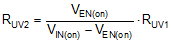
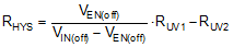
Choose RUV1 as 10 MΩ to minimize input quiescent current. Given the desired input voltage UVLO thresholds of 16 V and 14.5 V, calculate the resistance of RUV2 and RHYS as 825 kΩ and 37.4 kΩ, respectively. See Section 7.3.7 for more detail.