SNIS121J June 1999 – November 2016 LM61
PRODUCTION DATA.
- 1 Features
- 2 Applications
- 3 Description
- 4 Revision History
- 5 Pin Configuration and Functions
- 6 Specifications
- 7 Detailed Description
- 8 Application and Implementation
- 9 Power Supply Recommendations
- 10Layout
- 11Device and Documentation Support
- 12Mechanical, Packaging, and Orderable Information
Package Options
Mechanical Data (Package|Pins)
Thermal pad, mechanical data (Package|Pins)
Orderable Information
7 Detailed Description
7.1 Overview
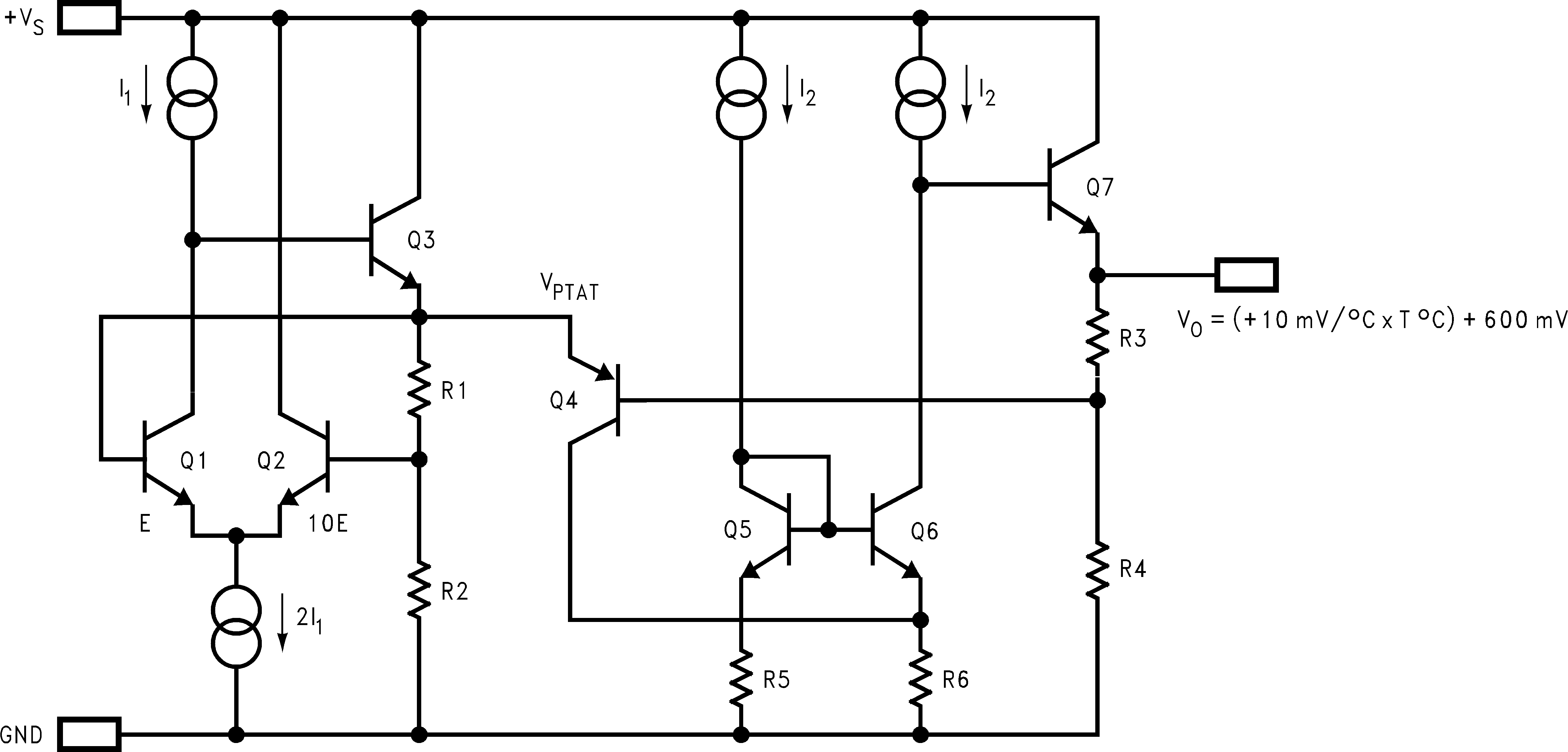
The LM61 is a precision integrated-circuit temperature sensor that can sense a –30°C to 100°C temperature range using a single positive supply. The output voltage of the LM61 has a positive temperature slope of
10 mV/°C. A 600-mV offset is included, enabling negative temperature sensing when biased by a single supply. The temperature-sensing element is comprised of a delta-VBE architecture. The temperature-sensing element is then buffered by an amplifier and provided to the VOUT pin. The amplifier has a simple class A output stage as shown in Functional Block Diagram.
7.2 Functional Block Diagram

7.3 Feature Description
7.3.1 LM61 Transfer Function
The LM61 follows a simple linear transfer function to achieve the accuracy as listed in Electrical Characteristics. Use Equation 1 to calculate the value of VO.
where
- T is the temperature in °C
- VO is the LM61 output voltage
7.4 Device Functional Modes
The only functional mode of the LM61 device is an analog output directly proportional to temperature.