SNVS754L January 2000 – June 2020 LM78L
PRODUCTION DATA.
- 1 Features
- 2 Applications
- 3 Description
- 4 Revision History
- 5 Device Comparison Table
- 6 Pin Configuration and Functions
-
7 Specifications
- 7.1 Absolute Maximum Ratings
- 7.2 ESD Ratings
- 7.3 Recommended Operating Conditions
- 7.4 Thermal Information
- 7.5 Electrical Characteristics — LM78L05
- 7.6 Electrical Characteristics — LM78L09
- 7.7 Electrical Characteristics — LM78L12
- 7.8 Electrical Characteristics — LM78L15
- 7.9 Electrical Characteristics — LM78L62
- 7.10 Typical Characteristics
- 8 Detailed Description
- 9 Application and Implementation
- 10Power Supply Recommendations
- 11Layout
- 12Device and Documentation Support
- 13Mechanical, Packaging, and Orderable Information
Package Options
Mechanical Data (Package|Pins)
Thermal pad, mechanical data (Package|Pins)
Orderable Information
9.2.2 Other Application Circuits
Figure 10 to Figure 14 show application circuit examples using the LM78Lxx devices. Customers must fully validate and test these circuits before implementing a design based on these examples. Unless otherwise noted, the design procedures in Fixed Output Regulator are applicable to these designs.
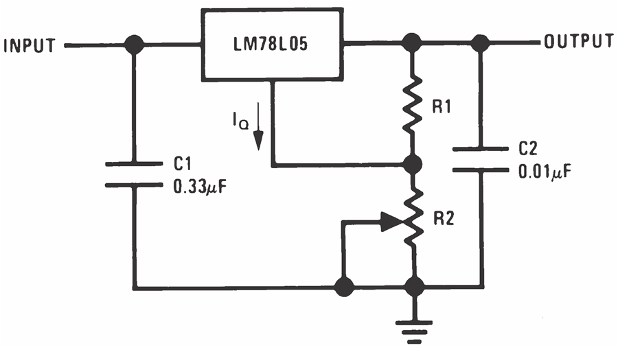
VO = 5 V + (5 V / R1 + IQ) × R2*
* The 5 V represents the fixed output voltage of the LM78L05. If using one of the other LM78Lxx devices, use that fixed output voltage value when calculating VO.
IQ < 5 V / (3 × R1)
Load regulation (LR) of LM78L05 ≈ (R1 + R2) / R1
Figure 10. Adjustable Output Regulator Circuit 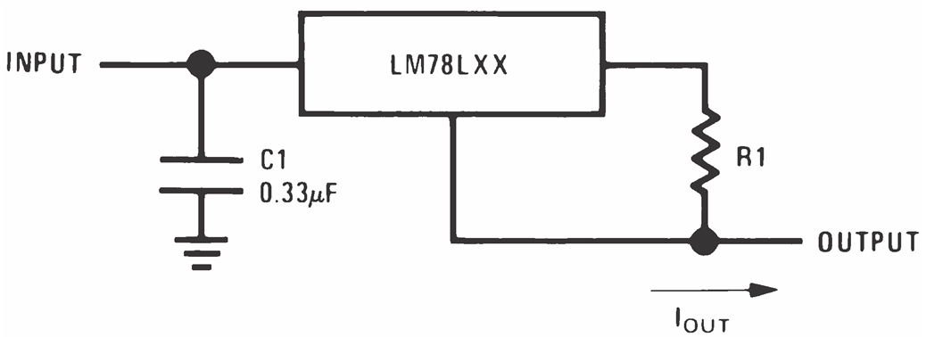
IOUT = (VO / R1) + IQ
IQ = 1.5 mA over line and load changes
Figure 11. Current Regulator Circuit 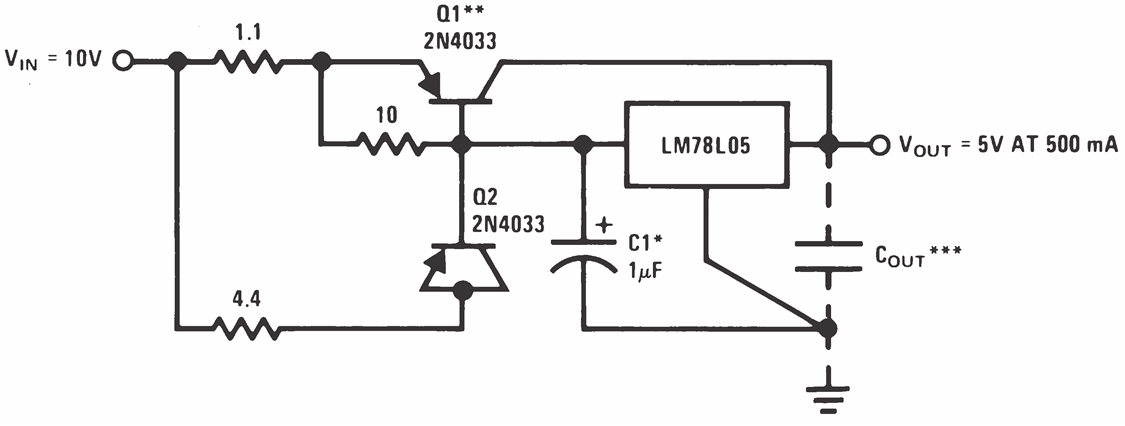
*Solid tantalum
**Heat sink Q1
***Optional: Improves ripple rejection and transient response.
Load Regulation = 0.6%, IL = 0 mA to 250 mA pulsed with tON = 50 ms.
Figure 12. 5-V, 500-mA Regulator With Short-Circuit Protection Circuit 
*Solid tantalum
Figure 13. ±15-V, 100-mA Dual Power Supply Circuit 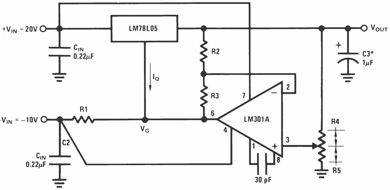
*Solid tantalum
VO = VG + 5 V, R1 = (–VIN / IQ(LM78L05))
VO = 5 V (R2 / R4) for (R2 + R3) = (R4 + R5)
A 0.5-V output will correspond to (R2 / R4) = 0.1, (R3 / R4) = 0.9
Figure 14. Variable Output Regulator Circuit (0.5 V to 18 V)