SNOSD37B march 2017 – april 2023 LMG1205
PRODUCTION DATA
- 1 Features
- 2 Applications
- 3 Description
- 4 Revision History
- 5 Pin Configuration and Functions
- 6 Specifications
- 7 Detailed Description
- 8 Application and Implementation
- 9 Power Supply Recommendations
- 10Layout
- 11Device and Documentation Support
Package Options
Mechanical Data (Package|Pins)
- YFX|12
Thermal pad, mechanical data (Package|Pins)
Orderable Information
3 Description
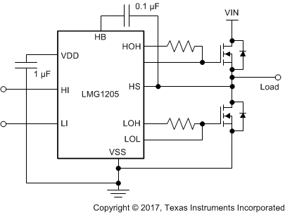
The LMG1205 is designed to drive both the high-side and the low-side enhancement mode Gallium Nitride (GaN) FETs in a synchronous buck, boost, or half-bridge configuration. The device has an integrated 100-V bootstrap diode and independent inputs for the high-side and low-side outputs for maximum control flexibility. The high-side bias voltage is generated using a bootstrap technique and is internally clamped at 5 V, which prevents the gate voltage from exceeding the maximum gate-source voltage rating of enhancement mode GaN FETs. The inputs of the LMG1205 are TTL logic compatible and can withstand input voltages up to 14 V regardless of the VDD voltage. The LMG1205 has split-gate outputs, providing flexibility to adjust the turnon and turnoff strength independently.
In addition, the strong sink capability of the LMG1205 maintains the gate in the low state, preventing unintended turnon during switching. The LMG1205 can operate up to several MHz. The LMG1205 is available in a 12-pin DSBGA package that offers a compact footprint and minimized package inductance.
| PART NUMBER | PACKAGE | BODY SIZE (NOM) |
|---|---|---|
| LMG1205 | DSBGA (12) | 2.00 mm × 2.00 mm |
 Simplified Application Diagram