SNLS308G April 2009 – June 2015 LMH0384
PRODUCTION DATA.
- 1 Features
- 2 Applications
- 3 Description
- 4 Revision History
- 5 Pin Configuration and Functions
- 6 Specifications
- 7 Detailed Description
- 8 Application and Implementation
- 9 Power Supply Recommendations
- 10Layout
- 11Device and Documentation Support
- 12Mechanical, Packaging, and Orderable Information
Package Options
Mechanical Data (Package|Pins)
- RUM|16
Thermal pad, mechanical data (Package|Pins)
- RUM|16
Orderable Information
7 Detailed Description
7.1 Overview
The LMH0384 3-Gbps HD - SD SDI Extended Reach and Configurable Adaptive Cable Equalizer is designed to equalize data transmitted over cable (or any media with similar dispersive loss characteristics). The equalizer operates over a wide range of data rates from 125 Mbps to 2.97 Gbps and supports ST 424, ST 292, ST 344, and ST 259 standards. The LMH0384 includes active sensing features and design enhancements including longer cable equalization, lower output jitter, configurable pin mode and SPI modes, a power-saving sleep mode, and programmable output common-mode voltage and swing. The LMH0384 implements DC restoration to correctly handle pathological data conditions.
7.2 Functional Block Diagram
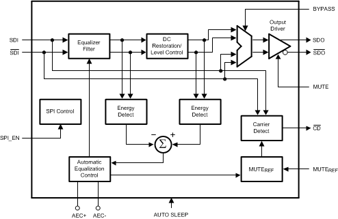
 Figure 6. Pin Mode
7.3 Feature Description
7.3.1 Block Description
The Equalizer Filter block is a multistage adaptive filter. If BYPASS is high, the equalizer filter is disabled.
The DC Restoration / Level Control block receives the differential signals from the equalizer filter block. This block incorporates a self-biasing DC restoration circuit to fully DC restore the signals. If BYPASS is high, this function is disabled.
The signals before and after the DC Restoration / Level Control block are used to generate the Automatic Equalization Control (AEC) signal. This control signal sets the gain and bandwidth of the equalizer filter. The loop response in the AEC block is controlled by an external 1-µF capacitor placed across the AEC+ and AEC- pins.
The Carrier Detect block generates the carrier detect signal based on the SDI input and an adjustment from the Mute Reference block.
The SPI Control block uses the MOSI, MISO, SCK, and SS signals in SPI mode to control the SPI registers. SPI_EN selects between SPI mode and pin mode. In pin mode, SPI_EN is driven logic low.
The Output Driver produces SDO and SDO.
7.3.2 Mute Reference (MUTEREF)
The mute reference sets the threshold for CD and (with CD tied to MUTE) determines the amount of cable to equalize before automatically muting the outputs. This is set by applying a voltage inversely proportional to the length of cable to equalize. The applied voltage must be greater than the MUTEREF floating voltage (typically 1.3 V) in order to change the CD threshold. As the applied MUTEREF voltage is increased, the amount of cable that can be equalized before carrier detect is deasserted and the outputs are muted is decreased. MUTEREF may be left unconnected or connected to ground for normal CD operation.
7.3.3 Carrier Detect (CD) and Mute
Carrier detect CD indicates if a valid signal is present at the LMH0384 input. If MUTEREF is used, the carrier detect threshold will be altered accordingly. CD provides a high voltage when no signal is present at the LMH0384 input. CD is low when a valid input signal is detected.
MUTE can be used to manually mute or enable SDO and SDO. Applying a high input to MUTE will mute the LMH0384 outputs by forcing the output to a logic zero. Applying a low input will force the outputs to be active.
CD and MUTE may be tied together to automatically mute the output when no input signal is present.
7.3.4 Auto Sleep
The auto sleep mode allows the LMH0384 to power down when no input signal is detected. If the AUTO SLEEP pin is set high, the LMH0384 goes into a deep power save mode when no signal is detected. The device powers on again once an input signal is detected. The auto sleep functionality can be turned off by setting AUTO SLEEP low or tying this pin to ground. An additional auto sleep setting available in SPI mode can be used to force the equalizer to power down regardless of whether there is an input signal or not. Auto sleep has precedence over mute and bypass modes.
In auto sleep mode, the time to power down the equalizer when the input signal is removed is less than 200 µs and should not have any impact on the system timing requirements. The device will wake up automatically once an input signal is detected (within 1 μs). The overall system will be limited only by the settling time constant of the equalizer adaptation loop.
7.3.5 Input Interfacing
The LMH0384 accepts either differential or single-ended input. The input must be AC-coupled. Functional Block Diagram shows the typical configuration for a single-ended input. The unused input must be properly terminated as shown.
The LMH0384 can be optimized for different launch amplitudes through the SPI (see Launch Amplitude Optimization in Programming).
The LMH0384 correctly handles equalizer pathological signals for standard definition and high definition serial digital video, as described in SMPTE RP 178 and RP 198, respectively.
7.3.6 Output Interfacing
SDO and SDO together are internally terminated 100-Ω LVDS outputs. These outputs can be DC coupled to most common differential receivers.
The default output common-mode voltage (VOS) is 1.25 V. The output common-mode voltage may be adjusted through the SPI in 200-mV increments, from 1.05 V to 1.85 V (see Output Driver Adjustments in Programming). This adjustable output common-mode voltage offers flexibility for interfacing to many types of receivers.
The default differential output swing (VSSP-P) is 700 mVP-P. The differential output swing may be adjusted through the SPI in 100 mV increments from 400 mVP-P to 800 mVP-P (see Output Driver Adjustments in Programming).
The LMH0384 output should be DC coupled to the input of the receiving device as long as the common-mode ranges of both devices are compatible. 100-Ω differential transmission lines should be used to connect between the LMH0384 outputs and the input of the receiving device where possible. Figure 7 shows an example of a DC-coupled interface between the LMH0384 and LMH0346 SDI reclocker. All that is required is the 100-Ω differential termination as shown. The resistor should be placed as close as possible to the LMH0346 input. If desired, this network may be terminated with two 50-Ω resistors and a center tap capacitor to ground in place of the signal 100-Ω resistor.
Figure 8 shows an example of a DC-coupled interface between the LMH0384 and LMH0356 SDI reclocker. The LMH0356 inputs have 50-Ω internal terminations (100-Ω differential) to terminate the transmission line, so no additional components are required.
The LMH0384 allows flexibility when interfacing to low voltage crosspoint switches (that is, 1.8 V) and other devices with limited input ranges. The LMH0384 outputs can be DC coupled to these devices in most cases, avoiding the need to AC couple.
The LMH0384 may be AC-coupled to the receiving device when necessary. For example, the LMH0384 outputs are not strictly compatible with 3.3 V CML and thus should not be connected through 50-Ω resistors to 3.3 V. If the input common-mode range of the receiving device is not compatible with the output common-mode range of the LMH0384, then AC coupling is required. Following the AC-coupling capacitors, the signal may have to be biased at the input of the receiving device.
 Figure 7. DC Output Interface to LMH0346 Reclocker
 Figure 8. DC Output Interface to LMH0356 Reclocker
7.4 Device Functional Modes
The LMH0384 supports two modes of operation: Pin and SPI Mode. In pin mode the LMH0384 is footprint compatible with the LMH0344 and legacy SDI equalizers. In the optional SPI mode, the LMH0384 provides register access to all of its features along with a cable length indicator, programmable output common-mode voltage and swing, and launch amplitude optimization.
7.5 Programming
Setting SPI_EN high enables the optional SPI register access mode. In SPI mode, the LMH0384 provides register access to all of its features along with a cable length indicator, programmable output common-mode voltage and swing, and launch amplitude optimization. There are five supported 8-bit registers in the device (see Table 1). With SPI_EN set low, the device operates in pin mode and is footprint compatible with the LMH0344, LMH0044, and LMH0074.
7.5.1 SPI Write
The SPI write is shown in Figure 2. The MOSI payload consists of a “0” (write command), seven address bits, and eight data bits. The SS signal is driven low, and the 16 bits are sent to the LMH0384's MOSI input. Data is latched on the rising edge of SCK. The MISO output is normally tri-stated during this operation. After the SPI write, SS must return high.
7.5.2 SPI Read
The SPI read is shown in Figure 3. The MOSI payload consists of a “1” (read command) and seven address bits. The SS signal is driven low, and the eight bits are sent to the LMH0384's MOSI input. The addressed location is accessed immediately after the rising edge of the 8th clock and the eight data bits are shifted out on MISO starting with the falling edge of the 8th clock. MOSI must be tri-stated immediately after the rising edge of the 8th clock. After the SPI read, SS must return high.
7.5.3 Output Driver Adjustments
The output driver swing (amplitude) and offset voltage (common-mode voltage) are adjustable through SPI register 01h.
The output swing is adjustable through bits [7:5] of SPI register 01h. The default value for these register bits is “011” for a peak to peak differential output voltage of 700 mVP-P. The output swing can be adjusted in 100 mV increments from 400 mVP-P to 800 mVP-P.
The offset voltage is adjustable through bits [4:2] of SPI register 01h. The default value for these register bits is “001” for an output offset of 1.25 V. The output common-mode voltage may be adjusted in 200-mV increments, from 1.05 V to 1.85 V. It can also be set to “101” for the maximum offset voltage. At this maximum offset voltage setting, the outputs are referenced to the positive supply and the offset voltage is around 2.1 V.
7.5.4 Launch Amplitude Optimization
The LMH0384 can compensate for attenuation of the input signal prior to the equalizer. This compensation is useful for applications with a passive splitter at the equalizer input or a non-ideal input termination network, and is controlled by SPI register 02h.
Bit 7 of SPI register 02h is used for coarse control of the launch amplitude setting. At the default setting of “0”, the LMH0384 operates normally and expects a launch amplitude of 800 mVP-P. Bit 7 may be set to “1” to optimize the LMH0384 for input signals with 6 dB of attenuation (400 mVP-P).
Once the coarse control is set, the LMH0384 input compensation may be further fine tuned by bits [6:3] of SPI register 02h. These bits may be used to tweak the input gain stage -22% to +40% around the coarse control setting.
7.5.5 Cable Length Indicator (CLI)
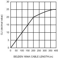
The Cable Length Indicator (CLI) provides an indication of the length of cable attached to the input. CLI is accessible through bits [7:3] of SPI register 03h. The 5-bit CLI ranges in decimal value from 0 to 25 (“00000” to “11001” binary) and increases as the cable length is increased. Figure 9 shows typical CLI values vs. Belden 1694A cable length. CLI is valid for Belden 1694A cable lengths of up to 140 m at 2.97 Gbps, 200 m at 1.485 Gbps, and 400 m at 270 Mbps.
 Figure 9. CLI vs. Belden 1694A Cable Length
7.5.6 Application of CLI: Extending 3G Reach
An application of CLI is to extend the 3G reach in systems which have margin in the jitter budget. This allows for additional cable reach at 2.97 Gbps at the expense of slightly higher output jitter. The extended 3G reach mode provides 15m of additional Belden 1694A cable reach, with an increase of output jitter at this longer cable length of 0.05 to 0.1 UI.
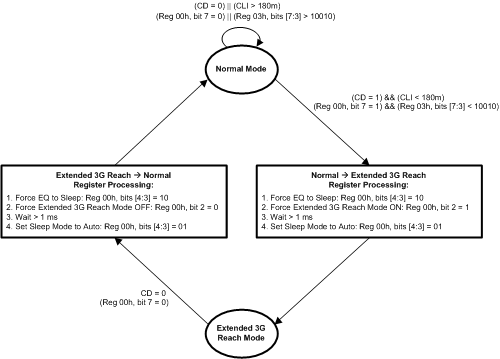
The extended 3G reach mode is accessible through bit 2 of SPI register 00h. In order to achieve longer 3G cable reach while still maintaining the performance at HD and SD data rates, a state machine can be implemented as shown in Figure 10. (Note: If this procedure is not followed, the maximum equalizable cable lengths for HD and SD data rates will be limited to less than what can be achieved in normal mode).
 Figure 10. Extended 3G Reach Mode State Machine Example
7.5.7 Explanation of Extended 3G Reach Mode State Machine (Figure 10)
When the LMH0384 is powered on, it will be in normal mode. If there is no input signal (register 00h, bit 7 = 0) or if the input cable is longer than a user programmable cable length (that is 180m, which means register 03h, bits [7:3] > 10010), then the device should remain in normal mode.
Once an input signal is detected (register 00h, bit 7 = 1) AND the detected cable length is shorter than the user programmed cable length of 180m (register 03h, bits [7:3] < 10010), then the equalizer can enter the extended 3G reach mode to allow for longer cable lengths at 2.97 Gbps. This requires the following procedure:
- Force the equalizer to sleep by writing “10” to bits [4:3] of register 00h.
- Turn on the extended 3G reach mode by writing “1” to bit 2 of register 00h.
- Wait at least 1ms.
- Set the sleep mode to auto by writing “01” to bits [4:3] of register 00h. Alternately, sleep mode may be set to off by writing “00” to bits [4:3] of register 00h.
The equalizer remains in extended 3G reach mode until the cable length is changed. If the cable length is changed, the input signal drops out momentarily. Once this happens (register 00h, bit 7 = 0), then the following procedure must be used to set the device back to normal mode:
- Force the equalizer to sleep by writing “10” to bits [4:3] of register 00h.
- Turn off the extended 3G reach mode by writing “0” to bit 2 of register 00h.
- Wait at least 1ms.
- Set the sleep mode to auto by writing “01” to bits [4:3] of register 00h. Alternately, sleep mode may be set to off by writing “00” to bits [4:3] of register 00h.