SNLS309I April 2010 – December 2014 LMH1983
PRODUCTION DATA.
- 1 Features
- 2 Applications
- 3 Description
- 4 Revision History
- 5 Description (continued)
- 6 Pin Configurations and Functions
- 7 Specifications
-
8 Detailed Description
- 8.1 Overview
- 8.2 Functional Block Diagram
- 8.3
Feature Description
- 8.3.1 Control of PLL1
- 8.3.2 PLL1 Loop Response Design Equations
- 8.3.3 Control of PLL2 and PLL3
- 8.3.4 Control of PLL4
- 8.3.5 Clock Output Jitter
- 8.3.6 Lock Determination
- 8.3.7 Lock Time Considerations
- 8.3.8 LOR Determination
- 8.3.9 Output Driver Adjustments
- 8.3.10 TOF1 Alignment
- 8.3.11 TOF2 and TOF3 Alignment
- 8.3.12 TOF4 Alignment
- 8.4 Device Functional Modes
- 8.5 Programming
- 8.6 Register Map
- 9 Applications and Implementation
- 10Power Supply Recommendations
- 11Layout
- 12Device and Documentation Support
- 13Mechanical, Packaging, and Orderable Information
Package Options
Mechanical Data (Package|Pins)
- RTA|40
Thermal pad, mechanical data (Package|Pins)
- RTA|40
Orderable Information
6 Pin Configurations and Functions
RTA40A Package
40-Pin WQFN Package with Exposed Thermal Pad
Top View
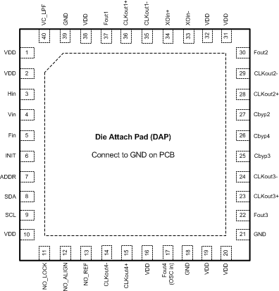
Pin Functions
| PIN | I/O | SIGNAL LEVEL |
DESCRIPTION | |
|---|---|---|---|---|
| NO. | NAME | |||
| 1 | VDD | – | Power | 3.3-V supply for PLL1 |
| 2 | VDD | – | Power | 3.3-V supply for logic I/O |
| 3 | Hin | I | LVCMOS | Horizontal sync reference signal Auto polarity correction for HVF will be based off Hin polarity. Recognized clock inputs can be applied to Hin. |
| 4 | Vin | I | LVCMOS | Vertical sync reference signal |
| 5 | Fin | I | LVCMOS | Field sync (odd/even) reference signal |
| 6 | INIT | I | LVCMOS | Reset signal for audio-video phase alignment (rising edge triggered) |
| 7 | ADDR | I | LVCMOS | I2C address select Pin settings: – Tie low: 0x65 (7-bit slave address in hex) – Float: 0x66 – Tie high: 0x67 |
| 8 | SDA(1) | I/O | I2C | I2C Data signal |
| 9 | SCL(1) | I | I2C | I2C Clock signal |
| 10 | VDD | – | Power | 3.3-V supply for logic I/O |
| 11 | NO_LOCK(2) | O | LVCMOS | Loss of lock status flag for PLLs 1-4 (active high) |
| 12 | NO_ALIGN | O | LVCMOS | Loss of alignment status flag for OUTs 1–4 (active high) |
| 13 | NO_REF | O | LVCMOS | Loss of reference status flag (active high) |
| 14 15 |
CLKout4– CLKout4+ |
O | LVDS | Audio clock from PLL4 (fundamental rate is 98.304 MHz). The output is 24.576 MHz by default and is selectable via the host. |
| 16 | VDD | – | Power | 3.3 V supply for CLKout4 |
| 17 | Fout4 (OSCin) | I/O | LVCMOS | Audio frame timing signal for OUT4 (active low.) Timing Generator fixed to PLL4 clock. The output is the audio-video-frame (AVF) pulse by default and is programmable via the host. Optional OSCin function can be used to apply a 27 MHz external clock for PLL4 to generate an audio clock independent of the video input reference; this function must be enabled via the host. |
| 18 | GND | – | GND | Ground |
| 19 | VDD | – | Power | 3.3 V supply for PLL3 and PLL4 |
| 20 | VDD | – | Power | 3.3 V supply for CLKout3 |
| 21 | GND | – | GND | Ground |
| 22 | Fout3 | O | LVCMOS | Video frame timing signal for OUT3 (active low). Timing generator assignable to PLL1, PLL2, or PLL3. OUT3 format is selectable via the host. |
| 23 24 |
CLKout3+ CLKout3– |
O | LVDS | Video clock from PLL1, PLL2, or PLL3 depending on output crosspoint mode. The output is 148.35 MHz by default and is selectable via the host. |
| 25 | Cbyp3 | – | Analog | Bias bypass for on-chip LDO for PLL3 Connect to 1.0 µF and 0.1 µF bypass capacitors. |
| 26 | Cbyp4 | – | Analog | Bias bypass for on-chip LDO for PLL4 Connect to 1.0 µF and 0.1 µF bypass capacitors. |
| 27 | Cbyp2 | – | Analog | Bias bypass for on-chip LDO for PLL2 Connect to 1.0 µF and 0.1 µF bypass capacitors. |
| 28 29 |
CLKout2+ CLKout2– |
O | LVDS | Video clock from PLL1, PLL2, or PLL3 depending on output crosspoint mode. The output is 148.5 MHz by default and is selectable via the host. |
| 30 | Fout2 | O | LVCMOS | Video frame timing signal for OUT2 (active low). Timing generator assignable to PLL1, PLL2, or PLL3. OUT2 format is selectable via the host. |
| 31 | VDD | – | Power | 3.3-V supply for CLKout2 |
| 32 | VDD | – | Power | 3.3-V supply for PLL2 |
| 33 34 |
XOin–(3)
XOin+ |
I | LVCMOS/LVDS | 27 MHz VCXO clock signal for PLL1. – LVCMOS: Directly connect clock signal to XOin+ and bias XOin- to mid-supply with 0.1µF bypass capacitor. – LVDS: Directly connect LVDS clock signals to XOin+ and XOin-.(4) |
| 35 36 |
CLKout1– CLKout1+ |
O | LVDS | Video clock from PLL1. The output is 27 MHz by default and is selectable via the host. |
| 37 | Fout1 | O | LVCMOS | Reference frame timing signal for OUT1 (active Low). Timing generator fixed to PLL1 OUT1 Format follows the reference input format. |
| 38 | VDD | – | Power | 3.3 V supply for CLKout1 |
| 39 | GND | – | GND | Ground |
| 40 | VC_LPF | O | Analog | Loop filter for PLL1 charge pump output with VCXO Voltage Control (VC) sensing. If free-run and holdover mode, PLL1 is disabled and an internal DAC outputs a control voltage to the VCXO. |
| – | DAP | – | GND | Die Attach Pad (Connect to ground on PCB) |
(1) SDA and SCL pins each require a pull-up resistor of 4.7 kΩ to the VDD supply.
(2) The NO_LOCK status flag is derived from the Lock Status register bits (LOCK1-4) for each PLL. Each lock status bit can be masked from the NO_LOCK flag by setting their respective mask bits.
(3) XOin must be driven by a 27 MHz clock in order to read or write registers via I2C.
(4) A TCXO or other clean 27 MHz oscillator can be applied for standalone clock generation using PLLs 2-4 (bypass PLL1).