SNOSAK9F June 2006 – June 2015 LMH6601 , LMH6601-Q1
PRODUCTION DATA.
- 1 Features
- 2 Applications
- 3 Description
- 4 Revision History
- 5 Pin Configuration and Functions
-
6 Specifications
- 6.1 Absolute Maximum Ratings
- 6.2 ESD Ratings - for LMH6601
- 6.3 ESD Ratings - for LMH6601-Q1
- 6.4 Recommended Operating Conditions
- 6.5 Thermal Information
- 6.6 Electrical Characteristics, 5 V
- 6.7 Electrical Characteristics, 3.3 V
- 6.8 Electrical Characteristics, 2.7 V
- 6.9 Switching Characteristics, 5 V
- 6.10 Switching Characteristics, 3.3 V
- 6.11 Switching Characteristics, 2.7 V
- 6.12 Typical Characteristics
- 7 Detailed Description
- 8 Application and Implementation
- 9 Power Supply Recommendations
- 10Layout
- 11Device and Documentation Support
- 12Mechanical, Packaging, and Orderable Information
Package Options
Mechanical Data (Package|Pins)
- DCK|6
Thermal pad, mechanical data (Package|Pins)
- DCK|6
Orderable Information
6 Specifications
6.1 Absolute Maximum Ratings(1)
| MIN | MAX | UNIT | ||
|---|---|---|---|---|
| VIN Differential | ±2.5 | V | ||
| Input Current(2) | ±10 | mA | ||
| Output Current | 200 mA(3) | mA | ||
| Supply Voltage (V+ – V−) | 6 | V | ||
| Voltage at Input/Output Pins | V++0.5, V−−0.5 | V | ||
| Junction Temperature | 150 | °C | ||
| Soldering Information | Infrared or Convection (20 sec.) | 235 | °C | |
| Wave Soldering (10 sec.) | 260 | |||
| Storage Temperature | −65 | 150 | °C | |
(1) Stresses beyond those listed under Absolute Maximum Ratings may cause permanent damage to the device. These are stress ratings only, which do not imply functional operation of the device at these or any other conditions beyond those indicated under Recommended Operating Conditions. Exposure to absolute-maximum-rated conditions for extended periods may affect device reliability.
(2) Negative input current implies current flowing out of the device.
(3) The maximum continuous output current (IOUT) is determined by device power dissipation limitations.
6.2 ESD Ratings - for LMH6601
| VALUE | UNIT | |||
|---|---|---|---|---|
| V(ESD) | Electrostatic discharge | Human body model (HBM), per ANSI/ESDA/JEDEC JS-001(1) | ±2000 | V |
| Charged-device model (CDM), per JEDEC specification JESD22-C101(2) | ±1000 | |||
(1) Human Body Model, applicable std. MIL-STD-883, Method 3015.7.
(2) JEDEC document JEP157 states that 250-V CDM allows safe manufacturing with a standard ESD control process.
6.3 ESD Ratings - for LMH6601-Q1
| VALUE | UNIT | |||
|---|---|---|---|---|
| V(ESD) | Electrostatic discharge | Human body model (HBM), per AEC Q100-002(1) | ±2000 | V |
| Charged-device model (CDM), per AEC Q100-011 | ±1000 | |||
(1) AEC Q100-002 indicates that HBM stressing shall be in accordance with the ANSI/ESDA/JEDEC JS-001 specification.
6.4 Recommended Operating Conditions(1)
| MIN | MAX | UNIT | ||
|---|---|---|---|---|
| Supply Voltage (V+ – V−) | 2.4 | 5.5 | V | |
| Operating Temperature | −40 | 85 | °C | |
(1) Stresses beyond those listed under Absolute Maximum Ratings may cause permanent damage to the device. These are stress ratings only, which do not imply functional operation of the device at these or any other conditions beyond those indicated under Recommended Operating Conditions. Exposure to absolute-maximum-rated conditions for extended periods may affect device reliability.
6.5 Thermal Information
| THERMAL METRIC(1) | LMH6601, LMH6601-Q1 | UNIT | |
|---|---|---|---|
| DCK (SC70) | |||
| 6 PINS | |||
| RθJA | Junction-to-ambient thermal resistance | 414 | °C/W |
(1) For more information about traditional and new thermal metrics, see the IC Package Thermal Metrics application report, SPRA953.
6.6 Electrical Characteristics, 5 V
Single-Supply with VS= 5 V, AV = +2, RF = 604 Ω, SD tied to V+, VOUT = VS/2, RL = 150 Ω to V− unless otherwise specified.(1)| PARAMETER | TEST CONDITIONS | MIN(3) | TYP(3) | MAX(3) | UNIT | ||
|---|---|---|---|---|---|---|---|
| FREQUENCY DOMAIN RESPONSE | |||||||
| SSBW | –3-dB Bandwidth Small Signal | VOUT = 0.25 VPP | 130 | MHz | |||
| SSBW_1 | VOUT = 0.25 VPP, AV = +1 | 250 | |||||
| Peak | Peaking | VOUT = 0.25 VPP, AV = +1 | 2.5 | dB | |||
| Peak_1 | Peaking | VOUT = 0.25 VPP | 0 | dB | |||
| LSBW | –3-dB Bandwidth Large Signal | VOUT = 2 VPP | 81 | MHz | |||
| Peak_2 | Peaking | VOUT = 2 VPP | 0 | dB | |||
| 0.1 dB BW | 0.1-dB Bandwidth | VOUT = 2 VPP | 30 | MHz | |||
| GBWP_1k | Gain Bandwidth Product | Unity Gain, RL = 1 kΩ to VS/2 | 155 | MHz | |||
| GBWP_150 | Unity Gain, RL = 150 Ω to VS/2 | 125 | |||||
| AVOL | Large Signal Open-Loop Gain | 0.5 V < VOUT < 4.5 V | 56 | 66 | dB | ||
| PBW | Full Power BW | –1 dB, AV = +4, VOUT = 4.2 VPP, RL = 150 Ω to VS/2 |
30 | MHz | |||
| DG | Differential Gain | 4.43 MHz, 1.7 V ≤ VOUT ≤ 3.3 V, RL = 150 Ω to V− |
0.06% | ||||
| DP | Differential Phase | 4.43 MHz, 1.7 V ≤ VOUT ≤ 3.3 V RL = 150 Ω to V− |
0.10 | deg | |||
| TIME DOMAIN RESPONSE | |||||||
| OS | Overshoot | 0.25-V Step | 10% | ||||
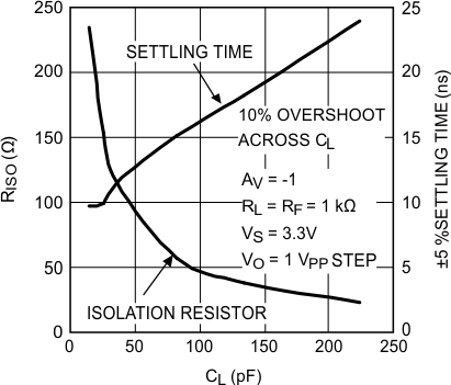
| CL | Capacitor Load Tolerance | AV = −1, 10% Overshoot, 75 Ω in Series | 50 | pF | |||
| DISTORTION and NOISE PERFORMANCE | |||||||
| HD2 | Harmonic Distortion (2nd) | 2 VPP, 10 MHz | −56 | dBc | |||
| HD2_1 | 4 VPP, 10 MHz, RL = 1 kΩ to VS/2 | −61 | |||||
| HD3 | Harmonic Distortion (3rd) | 2 VPP, 10 MHz | −73 | dBc | |||
| HD3_1 | 4 VPP, 10 MHz, RL = 1 kΩ to VS/2 | −64 | |||||
| THD | Total Harmonic Distortion | 4 VPP, 10 MHz, RL = 1 kΩ to VS/2 | −58 | ||||
| VN1 | Input Voltage Noise | >10 MHz | 7 | nV/√Hz | |||
| VN2 | 1 MHz | 10 | |||||
| IN | Input Current Noise | >1 MHz | 50 | fA/√Hz | |||
| STATIC, DC PERFORMANCE | |||||||
| VIO | Input Offset Voltage | ±1 | ±2.4 | mV | |||
| At temperature extremes | ±5 | ||||||
| DVIO | Input Offset Voltage Average Drift | See (4) | −5 | μV/°C | |||
| IB | Input Bias Current | See (5) | 5 | 50 | pA | ||
| IOS | Input Offset Current | See (5) | 2 | 25 | pA | ||
| RIN | Input Resistance | 0 V ≤ VIN ≤ 3.5 V | 10 | TΩ | |||
| CIN | Input Capacitance | 1.3 | pF | ||||
| +PSRR | Positive Power Supply Rejection Ratio | DC | 55 | 59 | dB | ||
| At temperature extremes | 51 | ||||||
| −PSRR | Negative Power Supply Rejection Ratio | DC | 53 | 61 | dB | ||
| At temperature extremes | 50 | ||||||
| CMRR | Common-Mode Rejection Ratio | DC | 56 | 68 | dB | ||
| At temperature extremes | 53 | ||||||
| CMVR | Input Voltage Range | CMRR > 50 dB (At temperature extremes) | V− – 0.20 | – | V+ – 1.5 | V | |
| ICC | Supply Current | Normal Operation VOUT = VS/2 |
9.6 | 11.5 | mA | ||
| At temperature extremes | 13.5 | ||||||
| Shutdown SD tied to ≤ 0.5 V (2) |
100 | nA | |||||
| VOH1 | Output High Voltage (Relative to V+) |
RL = 150 Ω to V– | –210 | –190 | mV | ||
| At temperature extremes | –480 | ||||||
| VOH2 | RL = 75 Ω to VS/2 | –190 | |||||
| VOH3 | RL = 10 kΩ to V– | –60 | –12 | ||||
| At temperature extremes | –110 | ||||||
| VOL1 | Output Low Voltage (Relative to V–) |
RL = 150 Ω to V– | 5 | 45 | mV | ||
| At temperature extremes | 125 | ||||||
| VOL2 | RL = 75 Ω to VS/2 | 120 | |||||
| VOL3 | RL = 10 kΩ to V– | 5 | 45 | ||||
| At temperature extremes | 125 | ||||||
| IO | Output Current | VOUT < 0.6 V from Respective Supply | Source | 150 | mA | ||
| Sink | 180 | ||||||
| IO_1 | VOUT = VS/2, VID = ±18 mV (6) |
±100 | |||||
| Load | Output Load Rating | THD < −30 dBc, f = 200 kHz, RL tied to VS/2, VOUT = 4 VPP |
20 | Ω | |||
| RO_Enabled | Output Resistance | Enabled, AV = +1 | 0.2 | Ω | |||
| RO_Disabled | Output Resistance | Shutdown | >100 | MΩ | |||
| CO_Disabled | Output Capacitance | Shutdown | 5 | pF | |||
| MISCELLANEOUS PERFORMANCE | |||||||
| VDMAX | Voltage Limit for Disable (Pin 5) | See (2) (At temperature extremes) | 0 | 0.5 | V | ||
| VDMIN | Voltage Limit for Enable (Pin 5) | See (2) (At temperature extremes) | 4.5 | 5 | V | ||
| Ii | Logic Input Current (Pin 5) | SD = 5 V(2) | 10 | pA | |||
| V_glitch | Turnon Glitch | 2.2 | V | ||||
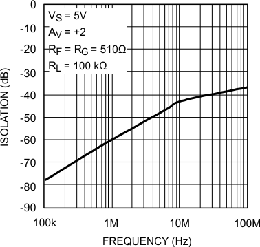
| IsolationOFF | Off Isolation | 1 MHz, RL = 1 kΩ | 60 | dB | |||
(1) Electrical Characteristics, 5 V values apply only for factory testing conditions at the temperature indicated. Factory testing conditions result in very limited self-heating of the device such that TJ = TA. No specification of parametric performance is indicated in the electrical tables under conditions of internal self-heating where TJ > TA.
(2) SD logic is CMOS compatible. To ensure proper logic level and to minimize power supply current, SD should typically be less than 10% of total supply voltage away from either supply rail.
(3) Typical values represent the most likely parametric norm as determined at the time of characterization. Actual typical values may vary over time and will also depend on the application and configuration. The typical values are not tested and are not ensured on shipped production material.
(4) Drift determined by dividing the change in parameter at temperature extremes by the total temperature change.
(5) This parameter is ensured by design and/or characterization and is not tested in production.
(6) “VID” is input differential voltage (input overdrive).
6.7 Electrical Characteristics, 3.3 V
Single-Supply with VS= 3.3 V, AV = +2, RF = 604Ω, SD tied to V+, VOUT = VS/2, RL = 150 Ω to V− unless otherwise specified.(1)| PARAMETER | TEST CONDITIONS | MIN(3) | TYP(3) | MAX(3) | UNIT | ||
|---|---|---|---|---|---|---|---|
| FREQUENCY DOMAIN RESPONSE | |||||||
| SSBW | –3-dB Bandwidth Small Signal | VOUT = 0.25 VPP | 125 | MHz | |||
| SSBW_1 | VOUT = 0.25 VPP, AV = +1 | 250 | |||||
| Peak | Peaking | VOUT = 0.25 VPP, AV = +1 | 3 | dB | |||
| Peak_1 | Peaking | VOUT = 0.25 VPP | 0.05 | dB | |||
| LSBW | –3-dB Bandwidth Large Signal | VOUT = 2 V PP | 75 | MHz | |||
| Peak_2 | Peaking | VOUT = 2 VPP | 0 | dB | |||
| 0.1 dB BW | 0.1-dB Bandwidth | VOUT = 2 VPP | 30 | MHz | |||
| GBWP_1k | Gain Bandwidth Product | Unity Gain, RL = 1 kΩ to VS/2 | 115 | MHz | |||
| GBWP_150 | Unity Gain, RL = 150 Ω to VS/2 | 105 | |||||
| AVOL | Large Signal Open-Loop Gain | 0.3 V < VOUT < 3 V | 56 | 67 | dB | ||
| PBW | Full Power BW | –1 dB, AV = +4, VOUT = 2.8 VPP, RL = 150 Ω to VS/2 |
30 | MHz | |||
| DG | Differential Gain | 4.43 MHz, 0.85 V ≤ VOUT ≤ 2.45 V, RL = 150 Ω to V− |
0.06% | ||||
| DP | Differential Phase | 4.43 MHz, 0.85 V ≤ VOUT ≤ 2.45 V RL = 150 Ω to V− |
0.23 | deg | |||
| TIME DOMAIN RESPONSE | |||||||
| OS | Overshoot | 0.25-V Step | 10% | ||||
| CL | Capacitor Load Tolerance | AV = −1, 10% Overshoot, 82 Ω in Series | 50 | pF | |||
| DISTORTION and NOISE PERFORMANCE | |||||||
| HD2 | Harmonic Distortion (2nd) | 2 VPP, 10 MHz | −61 | dBc | |||
| HD2_1 | 2 VPP, 10 MHz RL = 1 kΩ to VS/2 |
−79 | |||||
| HD3 | Harmonic Distortion (3rd) | 2 VPP, 10 MHz | −53 | dBc | |||
| HD3_2 | 2 VPP, 10 MHz RL = 1 kΩ to VS/2 |
−69 | |||||
| THD | Total Harmonic Distortion | 2 VPP, 10 MHz RL = 1 kΩ to VS/2 |
−66 | dBc | |||
| VN1 | Input Voltage Noise | >10 MHz | 7 | nV/√Hz | |||
| VN2 | 1 MHz | 10 | |||||
| IN | Input Current Noise | >1 MHz | 50 | fA/√Hz | |||
| STATIC, DC PERFORMANCE | |||||||
| VIO | Input Offset Voltage | ±1 | ±2.6 | mV | |||
| At temperature extremes | ±5.5 | ||||||
| DVIO | Input Offset Voltage Average Drift | See (4) | −4.5 | μV/°C | |||
| IB | Input Bias Current | See (5) | 5 | 50 | pA | ||
| IOS | Input Offset Current | See (5) | 2 | 25 | pA | ||
| RIN | Input Resistance | 0 V ≤ VIN ≤ 1.8 V | 15 | TΩ | |||
| CIN | Input Capacitance | 1.4 | pF | ||||
| +PSRR | Positive Power Supply Rejection Ratio | DC | 61 | 80 | dB | ||
| At temperature extremes | 51 | ||||||
| −PSRR | Negative Power Supply Rejection Ratio | DC | 57 | 72 | dB | ||
| At temperature extremes | 52 | ||||||
| CMRR | Common-Mode Rejection Ratio | DC | 58 | 73 | dB | ||
| At temperature extremes | 55 | ||||||
| CMVR | Input Voltage | CMRR > 50 dB (At temperature extremes) | V− – 0.20 | V+ – 1.5 | V | ||
| ICC | Supply Current | Normal Operation VOUT = VS/2 |
9.2 | 11 | mA | ||
| At temperature extremes | 13 | ||||||
| Shutdown: SD tied to ≤ 0.33 V(2) | 100 | nA | |||||
| VOH1 | Output High Voltage (Relative to V+) |
RL = 150 Ω to V– | –210 | –190 | mV | ||
| At temperature extremes | –360 | ||||||
| VOH2 | RL = 75 Ω to VS/2 | –190 | |||||
| VOH3 | RL = 10 kΩ to V− | –50 | –10 | ||||
| At temperature extremes | –100 | ||||||
| VOL1 | Output Low Voltage (Relative to V–) |
RL = 150 Ω to V– | 4 | 45 | mV | ||
| At temperature extremes | 125 | ||||||
| VOL2 | RL = 75 Ω to VS/2 | 105 | |||||
| VOL3 | RL = 10 kΩ to V– | 4 | 45 | ||||
| At temperature extremes | 125 | ||||||
| IO | Output Current | VOUT < 0.6 V from Respective Supply | Source | 50 | mA | ||
| Sink | 75 | ||||||
| IO_1 | VOUT = VS/2, VID = ±18 mV(6) | ±75 | |||||
| Load | Output Load Rating | THD < −30 dBc, f = 200 kHz, RL tied to VS/2, VOUT = 2.6 VPP |
25 | Ω | |||
| RO_Enabled | Output Resistance | Enabled, AV = +1 | 0.2 | Ω | |||
| RO_Disabled | Output Resistance | Shutdown | >100 | MΩ | |||
| CO_Disabled | Output Capacitance | Shutdown | 5.6 | pF | |||
| MISCELLANEOUS PERFORMANCE | |||||||
| VDMAX | Voltage Limit for Disable (Pin 5) | See (2) (At temperature extremes) | 0 | 0.33 | V | ||
| VDMIN | Voltage Limit for Enable (Pin 5) | See (2) (At temperature extremes) | 2.97 | 3.3 | V | ||
| Ii | Logic Input Current (Pin 5) | SD = 3.3 V(2) | 8 | pA | |||
| V_glitch | Turnon Glitch | 1.6 | V | ||||
| IsolationOFF | Off Isolation | 1 MHz, RL = 1 kΩ | 60 | dB | |||
(1) Electrical Characteristics, 3.3 V values apply only for factory testing conditions at the temperature indicated. Factory testing conditions result in very limited self-heating of the device such that TJ = TA. No specification of parametric performance is indicated in the electrical tables under conditions of internal self-heating where TJ > TA.
(2) SD logic is CMOS compatible. To ensure proper logic level and to minimize power supply current, SD should typically be less than 10% of total supply voltage away from either supply rail.
(3) Typical values represent the most likely parametric norm as determined at the time of characterization. Actual typical values may vary over time and will also depend on the application and configuration. The typical values are not tested and are not ensured on shipped production material.
(4) Drift determined by dividing the change in parameter at temperature extremes by the total temperature change.
(5) This parameter is ensured by design and/or characterization and is not tested in production.
(6) “VID” is input differential voltage (input overdrive).
6.8 Electrical Characteristics, 2.7 V
Single-Supply with VS = 2.7 V, AV = +2, RF = 604 Ω, SD tied to V+, VOUT = VS/2, RL = 150 Ω to V− unless otherwise specified.(1)| PARAMETER | TEST CONDITIONS | MIN(3) | TYP(3) | MAX(3) | UNIT | ||
|---|---|---|---|---|---|---|---|
| FREQUENCY DOMAIN RESPONSE | |||||||
| SSBW | –3-dB Bandwidth Small Signal | VOUT = 0.25 VPP | 120 | MHz | |||
| SSBW_1 | VOUT = 0.25 VPP, AV = +1 | 250 | |||||
| Peak | Peaking | VOUT = 0.25 VPP, AV = +1 | 3.1 | dB | |||
| Peak_1 | Peaking | VOUT = 0.25 VPP | 0.1 | dB | |||
| LSBW | –3-dB Bandwidth Large Signal | VOUT = 2 V PP | 73 | MHz | |||
| Peak_2 | Peaking | VOUT = 2 VPP | 0 | dB | |||
| 0.1 dB BW | 0.1-dB Bandwidth | VOUT = 2 VPP | 30 | MHz | |||
| GBWP_1k | Gain Bandwidth Product | Unity Gain, RL = 1 kΩ to VS/2 | 110 | MHz | |||
| GBWP_150 | Unity Gain, RL = 150 Ω to VS/2 | 81 | |||||
| AVOL | Large Signal Open-Loop Gain | 0.25 V < VOUT < 2.5 V | 56 | 65 | dB | ||
| PBW | Full Power BW | –1 dB, AV = +4, VOUT = 2 VPP, RL = 150 Ω to VS/2 |
13 | MHz | |||
| DG | Differential Gain | 4.43 MHz, 0.45 V ≤ VOUT ≤ 2.05 V RL = 150 Ω to V− |
0.12% | ||||
| DP | Differential Phase | 4.43 MHz, 0.45 V ≤ VOUT ≤ 2.05 V RL = 150 Ω to V− |
0.62 | deg | |||
| TIME DOMAIN RESPONSE | |||||||
| OS | Overshoot | 0.25-V Step | 10% | ||||
| DISTORTION and NOISE PERFORMANCE | |||||||
| HD2 | Harmonic Distortion (2nd) | 1 VPP, 10 MHz | −58 | dBc | |||
| HD3 | Harmonic Distortion (3rd) | 1 VPP, 10 MHz | −60 | dBc | |||
| VN1 | Input Voltage Noise | >10 MHz | 8.4 | nV/√Hz | |||
| VN2 | 1 MHz | 12 | |||||
| IN | Input Current Noise | >1 MHz | 50 | fA/√Hz | |||
| STATIC, DC PERFORMANCE | |||||||
| VIO | Input Offset Voltage | ±1 | ±3.5 | mV | |||
| At temperature extremes | ±6.5 | ||||||
| DVIO | Input Offset Voltage Average Drift | See (4) | −6.5 | μV/°C | |||
| IB | Input Bias Current | See (5) | 5 | 50 | pA | ||
| IOS | Input Offset Current | See (5) | 2 | 25 | pA | ||
| RIN | Input Resistance | 0V ≤ VIN ≤ 1.2V | 20 | TΩ | |||
| CIN | Input Capacitance | 1.6 | pF | ||||
| +PSRR | Positive Power Supply Rejection Ratio | DC | 58 | 68 | dB | ||
| At temperature extremes | 53 | ||||||
| −PSRR | Negative Power Supply Rejection Ratio | DC | 56 | 69 | dB | ||
| At temperature extremes | 53 | ||||||
| CMRR | Common-Mode Rejection Ratio | DC | 57 | 77 | dB | ||
| At temperature extremes | 52 | ||||||
| CMVR | Input Voltage | CMRR > 50 dB (At temperature extremes) | V− – 0.20 | – | V+ – 1.5 | V | |
| ICC | Supply Current | Normal Operation VOUT = VS/2 |
9 | 10.6 | mA | ||
| At temperature extremes | 12.5 | ||||||
| Shutdown SD tied to ≤ 0.27 V(2) |
100 | nA | |||||
| VOH1 | Output High Voltage (Relative to V+) |
RL = 150 Ω to V– | –260 | –200 | mV | ||
| At temperature extremes | –420 | ||||||
| VOH2 | RL = 75 Ω to VS/2 | –200 | |||||
| VOH3 | RL = 10 kΩ to V– | –50 | –10 | ||||
| At temperature extremes | 100 | ||||||
| VOL1 | Output Low Voltage (Relative to V–) |
RL = 150 Ω to V– | 4 | 45 | mV | ||
| 125 | |||||||
| VOL2 | RL = 75 Ω to VS/2 | 125 | |||||
| VOL3 | RL = 10 kΩ to V– | 4 | 45 | ||||
| At temperature extremes | 125 | ||||||
| IO | Output Current | VOUT ≤ 0.6 V from Respective Supply | Source | 25 | mA | ||
| Sink | 62 | ||||||
| IO_1 | VOUT = VS/2, VID = ±18 mV(6) | Source | 25 | ||||
| Sink | 35 | ||||||
| Load | Output Load Rating | THD < −30 dBc, f = 200 kHz, RL tied to VS/2, VOUT = 2.2 VPP | 40 | Ω | |||
| RO_Enable | Output Resistance | Enabled, AV = +1 | 0.2 | Ω | |||
| RO_Disabled | Output Resistance | Shutdown | >100 | MΩ | |||
| CO_Disabled | Output Capacitance | Shutdown | 5.6 | pF | |||
| MISCELLANEOUS PERFORMANCE | |||||||
| VDMAX | Voltage Limit for Disable (Pin 5) | See (2) (At temperature extremes) | 0 | 0.27 | V | ||
| VDMIN | Voltage Limit for Enable (Pin 5) | See (2) (At temperature extremes) | 2.43 | 2.7 | V | ||
| Ii | Logic Input Current (Pin 5) | SD = 2.7 V(2) | 4 | pA | |||
| V_glitch | Turnon Glitch | 1.2 | V | ||||
| IsolationOFF | Off Isolation | 1 MHz, RL = 1 kΩ | 60 | dB | |||
(1) Electrical Characteristics, 2.7 V values apply only for factory testing conditions at the temperature indicated. Factory testing conditions result in very limited self-heating of the device such that TJ = TA. No specification of parametric performance is indicated in the electrical tables under conditions of internal self-heating where TJ > TA.
(2) SD logic is CMOS compatible. To ensure proper logic level and to minimize power supply current, SD should typically be less than 10% of total supply voltage away from either supply rail.
(3) Typical values represent the most likely parametric norm as determined at the time of characterization. Actual typical values may vary over time and will also depend on the application and configuration. The typical values are not tested and are not ensured on shipped production material.
(4) Drift determined by dividing the change in parameter at temperature extremes by the total temperature change.
(5) This parameter is ensured by design and/or characterization and is not tested in production.
(6) “VID” is input differential voltage (input overdrive).
6.9 Switching Characteristics, 5 V
Single-Supply with VS= 5 V, AV = +2, RF = 604 Ω, SD tied to V+, VOUT = VS/2, RL = 150 Ω to V− unless otherwise specified.| PARAMETER | TEST CONDITIONS | MIN | TYP | MAX | UNIT | |
|---|---|---|---|---|---|---|
| TIME DOMAIN RESPONSE | ||||||
| TRS/TRL | Rise and Fall Time | 0.25-V Step | 2.6 | ns | ||
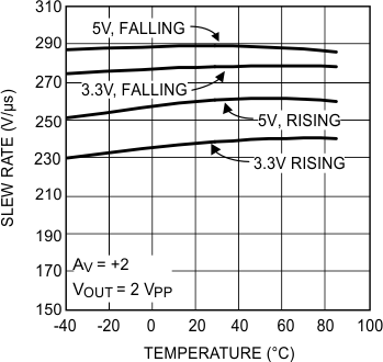
| SR | Slew Rate | 2-V Step | 275 | V/μs | ||
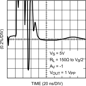
| TS | Settling Time | 1-V Step, ±0.1% | 50 | ns | ||
| TS_1 | 1-V Step, ±0.02% | 220 | ||||
| PD | Propagation Delay | Input to Output, 250-mV Step, 50% | 2.4 | ns | ||
| MISCELLANEOUS PERFORMANCE | ||||||
| Ton | Turnon Time | 1.4 | µs | |||
| Toff | Turnoff Time | 520 | ns | |||
| T_OL | Overload Recovery | <20 | ns | |||
6.10 Switching Characteristics, 3.3 V
Single-Supply with VS= 3.3 V, AV = +2, RF = 604Ω, SD tied to V+, VOUT = VS/2, RL = 150 Ω to V− unless otherwise specified.(1)| PARAMETER | TEST CONDITIONS | MIN | TYP | MAX | UNIT | |
|---|---|---|---|---|---|---|
| TIME DOMAIN RESPONSE | ||||||
| TRS/TRL | Rise and Fall Time | 0.25-V Step | 2.7 | ns | ||
| SR | Slew Rate | 2-V Step | 260 | V/μs | ||
| TS | Settling Time | 1-V Step, ±0.1% | 70 | ns | ||
| TS_1 | 1-V Step, ±0.02% | 300 | ||||
| PD | Propagation Delay | Input to Output, 250-mV Step, 50% | 2.6 | ns | ||
| MISCELLANEOUS PERFORMANCE | ||||||
| Ton | Turnon Time | 3.5 | µs | |||
| Toff | Turnoff Time | 500 | ns | |||
(1) Electrical Characteristics, 3.3 V values apply only for factory testing conditions at the temperature indicated. Factory testing conditions result in very limited self-heating of the device such that TJ = TA. No specification of parametric performance is indicated in the electrical tables under conditions of internal self-heating where TJ > TA.
6.11 Switching Characteristics, 2.7 V
Single-Supply with VS = 2.7 V, AV = +2, RF = 604 Ω, SD tied to V+, VOUT = VS/2, RL = 150 Ω to V− unless otherwise specified.(1)| PARAMETER | TEST CONDITIONS | MIN | TYP | MAX | UNIT | |
|---|---|---|---|---|---|---|
| TIME DOMAIN RESPONSE | ||||||
| TRS/TRL | Rise and Fall Time | 0.25-V Step | 2.7 | ns | ||
| SR | Slew Rate | 2-V Step | 260 | V/μs | ||
| TS | Settling Time | 1-V Step, ±0.1% | 147 | ns | ||
| TS_1 | 1-V Step, ±0.02% | 410 | ||||
| PD | Propagation Delay | Input to Output, 250-mV Step, 50% | 3.4 | ns | ||
| MISCELLANEOUS PERFORMANCE | ||||||
| Ton | Turnon Time | 5.2 | µs | |||
| Toff | Turnoff Time | 760 | ns | |||
(1) Electrical Characteristics, 2.7 V values apply only for factory testing conditions at the temperature indicated. Factory testing conditions result in very limited self-heating of the device such that TJ = TA. No specification of parametric performance is indicated in the electrical tables under conditions of internal self-heating where TJ > TA.
6.12 Typical Characteristics
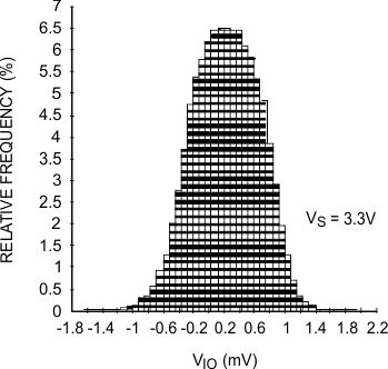
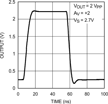
Unless otherwise noted, all data is with AV = +2, RF = RG = 604 Ω, VS = 3.3V, VOUT = VS/2, SD tied to V+, RL = 150 Ω to V−, T = 25°C.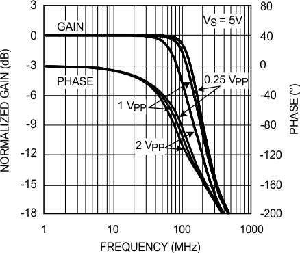
for Various Output Amplitudes
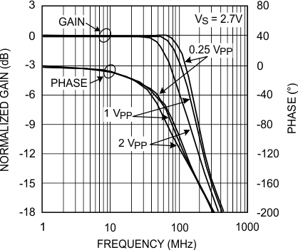
for Various Output Amplitudes
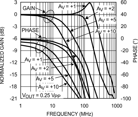
for Various Gain
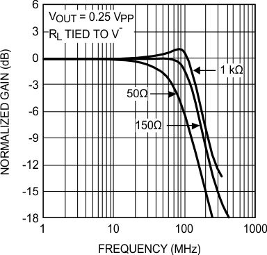
for Various Loads
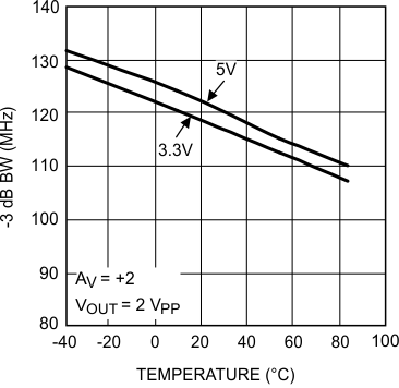
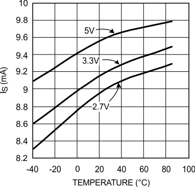
vs. Ambient Temperature
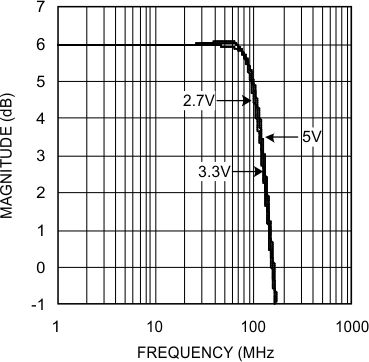
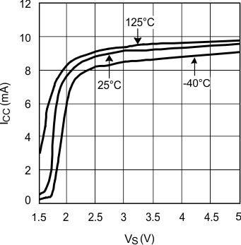
for Various Supply Voltage
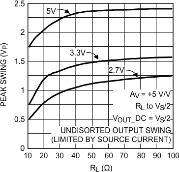
i.
Figure 13. Peak Output Swing vs. RL
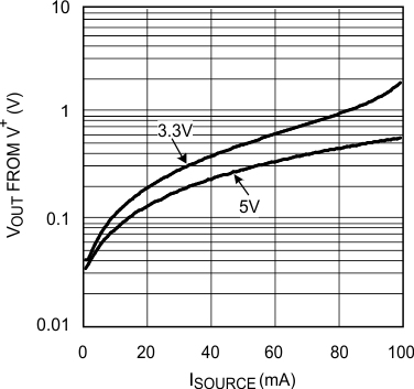
for Various Supply Voltages
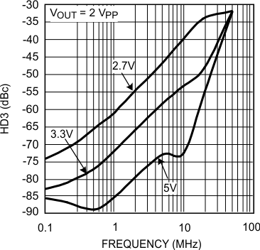
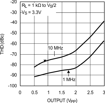
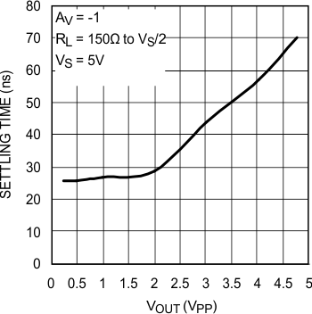
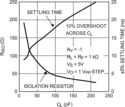
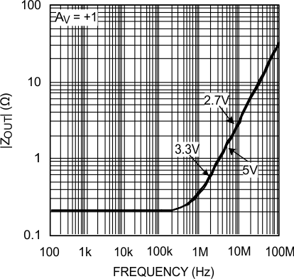
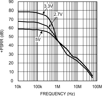
vs. Frequency for Various Supply Voltages
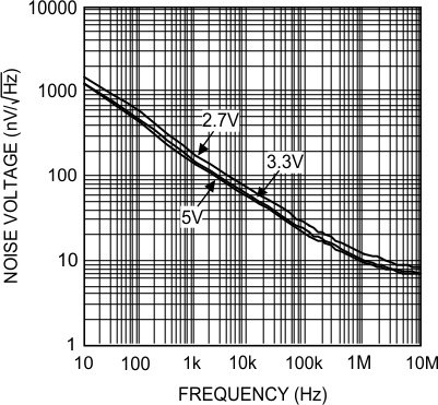
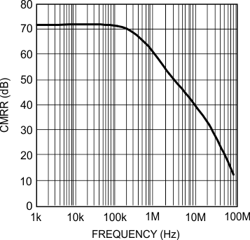
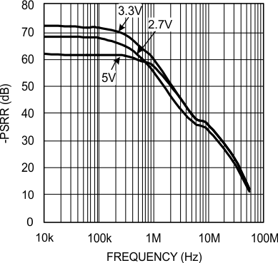
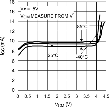
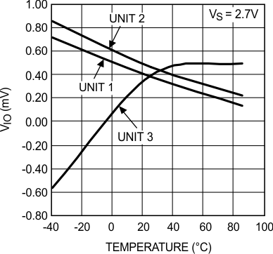
vs. Ambient Temperature for 3 Representative Units
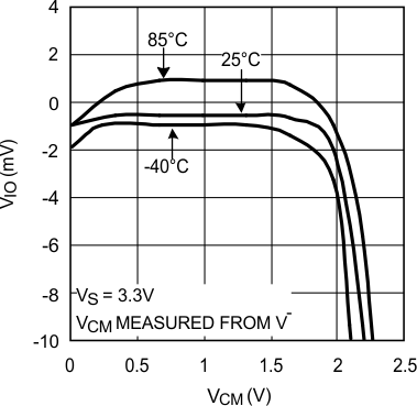
vs. VCM (Typical Part)
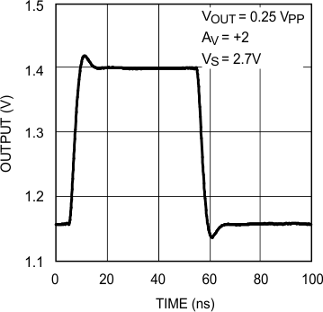
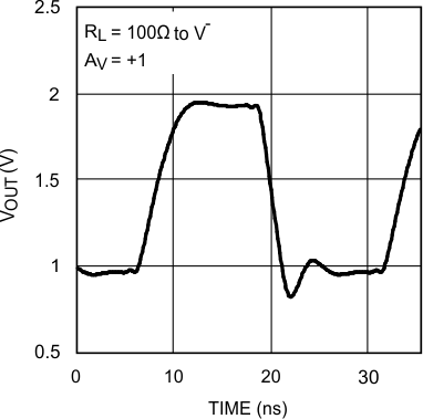
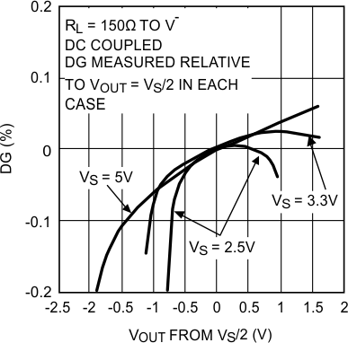
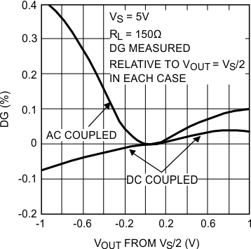
(DC- and AC-Coupled Load Compared)
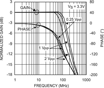
for Various Output Amplitudes
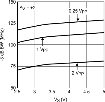
for Various Output Swings
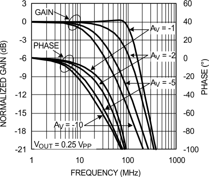
for Various Gain
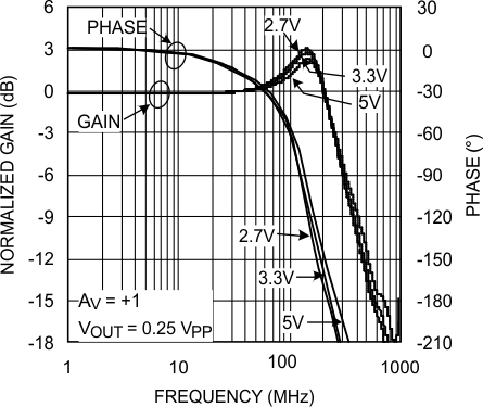
for Various Supply Voltages
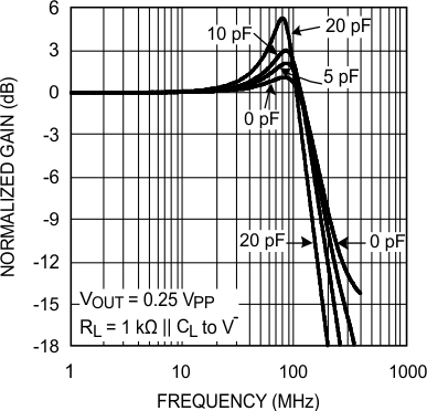
for Various Capacitor Load
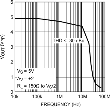
vs. Frequency
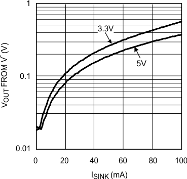
for Various Supply Voltages
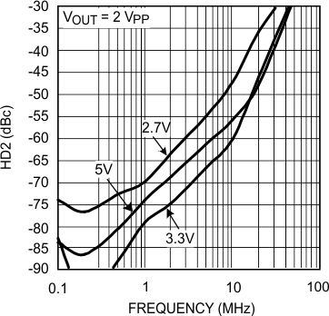
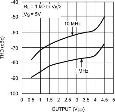
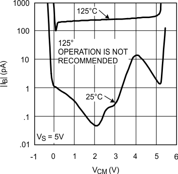
vs. Common Mode Voltage
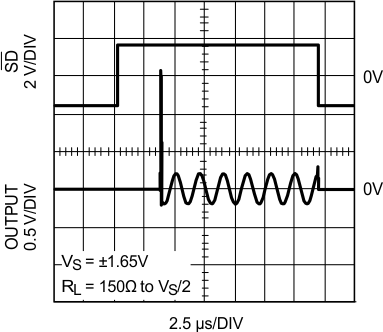
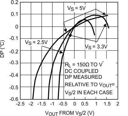
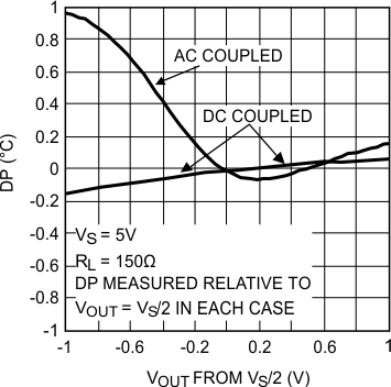
(DC- and AC-Coupled Load Compared)