SNAS635E December   2013  – January 2022 LMK00334

PRODUCTION DATA  

  1. Features
  2. Applications
  3. Description
  4. Revision History
  5. Pin Configuration and Functions
  6. Specifications
    1. 6.1 Absolute Maximum Ratings
    2. 6.2 ESD Ratings
    3. 6.3 Recommended Operating Conditions
    4. 6.4 Thermal Information
    5. 6.5 Electrical Characteristics
    6. 6.6 Timing Requirements, Propagation Delay, and Output Skew
    7. 6.7 Typical Characteristics
  7. Parameter Measurement Information
    1. 7.1 Differential Voltage Measurement Terminology
  8. Detailed Description
    1. 8.1 Overview
    2. 8.2 Functional Block Diagram
    3. 8.3 Feature Description
      1. 8.3.1 Crystal Power Dissipation vs. RLIM
      2. 8.3.2 Clock Inputs
      3. 8.3.3 Clock Outputs
        1. 8.3.3.1 Reference Output
    4. 8.4 Device Functional Modes
      1. 8.4.1 VCC and VCCO Power Supplies
  9. Application and Implementation
    1. 9.1 Application Information
    2. 9.2 Typical Application
      1. 9.2.1 Design Requirements
        1. 9.2.1.1 Driving the Clock Inputs
        2. 9.2.1.2 Crystal Interface
      2. 9.2.2 Detailed Design Procedure
        1. 9.2.2.1 Termination and Use of Clock Drivers
        2. 9.2.2.2 Termination for DC-Coupled Differential Operation
        3. 9.2.2.3 Termination for AC-Coupled Differential Operation
      3. 9.2.3 Application Curve
  10. 10Power Supply Recommendations
    1. 10.1 Current Consumption and Power Dissipation Calculations
      1. 10.1.1 Power Dissipation Example: Worst-Case Dissipation
    2. 10.2 Power Supply Bypassing
      1. 10.2.1 Power Supply Ripple Rejection
  11. 11Layout
    1. 11.1 Layout Guidelines
    2. 11.2 Layout Example
    3. 11.3 Thermal Management
  12. 12Device and Documentation Support
    1. 12.1 Documentation Support
      1. 12.1.1 Related Documentation
    2. 12.2 Receiving Notification of Documentation Updates
    3. 12.3 Support Resources
    4. 12.4 Trademarks
    5. 12.5 Electrostatic Discharge Caution
    6. 12.6 Glossary
  13. 13Mechanical, Packaging, and Orderable Information

Package Options

Mechanical Data (Package|Pins)
Thermal pad, mechanical data (Package|Pins)
Orderable Information

Description

The LMK00334 device is a 4-output HCSL fanout buffer intended for high-frequency, low-jitter clock, data distribution, and level translation. It is capable of distributing the reference clock for ADCs, DACs, multi-gigabit ethernet, XAUI, fibre channel, SATA/SAS, SONET/SDH, CPRI, and high-frequency backplanes.

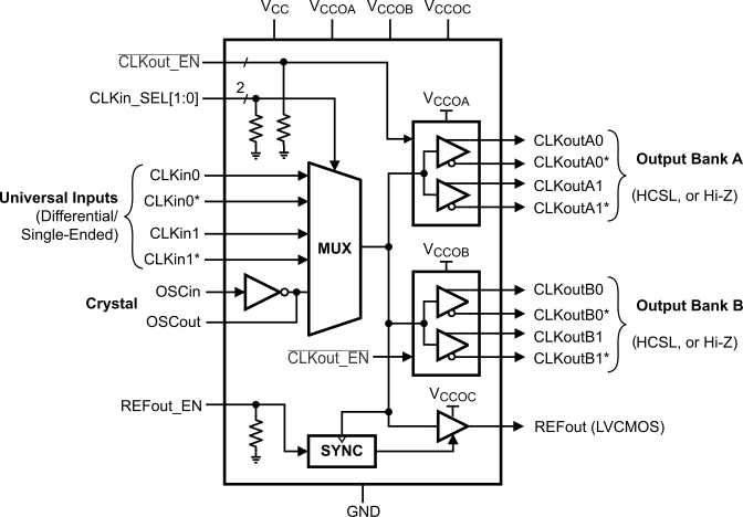
The input clock can be selected from two universal inputs or one crystal input. The selected input clock is distributed to two banks of two HCSL outputs and one LVCMOS output. The LVCMOS output has a synchronous enable input for runt-pulse-free operation when enabled or disabled. The LMK00334 operates from a 3.3-V core supply and three independent 3.3-V or 2.5-V output supplies.

The LMK00334 provides high performance, versatility, and power efficiency, making it ideal for replacing fixed-output buffer devices while increasing timing margin in the system.

Device Information(1)
PART NUMBERPACKAGEBODY SIZE (NOM)
LMK00334WQFN (32)5.00 mm × 5.00 mm
For all available packages, see the orderable addendum at the end of the data sheet.
GUID-6CB5C03A-3A34-4866-9217-CF4B09294208-low.gifLMK00334 Functional Block Diagram