SNAS691E December 2016 – December 2023 LMK62A2-100M , LMK62A2-150M , LMK62A2-156M , LMK62A2-200M , LMK62A2-266M , LMK62E0-156M , LMK62E2-100M , LMK62E2-156M , LMK62I0-100M , LMK62I0-156M
PRODUCTION DATA
- 1
- 1 Features
- 2 Applications
- 3 Description
- 4 Pin Configuration and Functions
-
5 Specifications
- 5.1 Absolute Maximum Ratings
- 5.2 ESD Ratings
- 5.3 Recommended Operating Conditions
- 5.4 Thermal Information
- 5.5 Electrical Characteristics - Power Supply
- 5.6 LVPECL Output Characteristics
- 5.7 LVDS Output Characteristics
- 5.8 HCSL Output Characteristics
- 5.9 OE Input Characteristics
- 5.10 Frequency Tolerance Characteristics
- 5.11 Power-On/Reset Characteristics (VDD)
- 5.12 PSRR Characteristics
- 5.13 PLL Clock Output Jitter Characteristics
- 5.14 Additional Reliability and Qualification
- 6 Parameter Measurement Information
- 7 Application and Implementation
- 8 Device and Documentation Support
- 9 Revision History
- 10Mechanical, Packaging, and Orderable Information
Package Options
Refer to the PDF data sheet for device specific package drawings
Mechanical Data (Package|Pins)
- SIA|6
Thermal pad, mechanical data (Package|Pins)
Orderable Information
6.1 Device Output Configurations
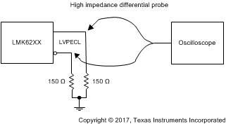
 Figure 6-1 LVPECL Output DC Configuration During Device Test
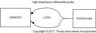
 Figure 6-2 LVDS Output DC Configuration During Device Test
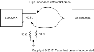
 Figure 6-3 HCSL Output DC Configuration During Device Test (1)
 Figure 6-4 LVPECL Output AC Configuration During Device Test
 Figure 6-5 LVDS Output AC Configuration During Device Test
 Figure 6-6 HCSL Output AC Configuration During Device Test
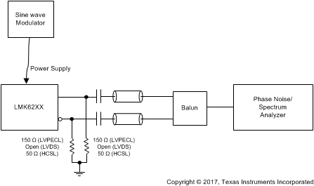
 Figure 6-7 PSRR Test Setup
 Figure 6-8 Differential Output Voltage and Rise/Fall Time
1. Also compatible with 85 Ω termination