SNOSCS3B September 2013 – March 2014 LMP91300
PRODUCTION DATA.
- 1 Features
- 2 Applications
- 3 Description
- 4 Revision History
- 5 Terminal Configuration and Functions
- 6 Specifications
-
7 Detailed Description
- 7.1 Overview
- 7.2 Functional Block Diagram
- 7.3 Feature Description
- 7.4 Device Functional Modes
- 7.5 Programming
- 7.6
Register Maps
- 7.6.1 DET_H_MSB_INIT - Detection High Threshold MSB (Initial) (Address 0x66)
- 7.6.2 DET_H_LSB_INIT - Detection High Threshold LSB (Initial) (Address 0x67)
- 7.6.3 DET_L_MSB_INIT - Detection Low Threshold MSB (Initial) (Address 0x68)
- 7.6.4 DET_L_LSB_INIT - Detection Low Threshold LSB (Initial) (Address 0x69)
- 7.6.5 INFO0 - Device Information 0 (Address 0x6A)
- 7.6.6 INFO1 - Device Information 1 (Address 0x6B)
- 7.6.7 INFO2 - Device Information 2 (Address 0x6C)
- 7.6.8 INFO3 - Device Information 3 (Address 0x6D)
- 7.6.9 OSC_CONFIG_0 - Oscillator Configuration 0 Register (Address 0x6E)
- 7.6.10 45
- 7.6.11 OSC_CONFIG_1 - Oscillator Configuration 1 Register (Address 0x6F)
- 7.6.12 OSC_CONFIG_2 - Oscillator Configuration 2 Register (Address 0x70)
- 7.6.13 OSC_CONFIG_3_INIT - Oscillator Configuration 3 Register (Initial) (Address 0x71)
- 7.6.14 OUT_CONFIG_INIT - Output Configuration Register (Initial) (Address 0x72)
- 7.6.15 DET_H_MSB_FNL - Detection High Threshold MSB (Final) (Address 0x73)
- 7.6.16 DET_H_LSB_FNL - Detection High Threshold LSB (Final) (Address 0x74)
- 7.6.17 DET_L_MSB_FNL - Detection Low Threshold MSB (Final) (Address 0x75)
- 7.6.18 DET_L_LSB_FNL - Detection Low Threshold LSB (Final) (Address 0x76)
- 7.6.19 OSC_CONFIG_3_FNL - Oscillator Configuration 3 Register (Final) (Address 0x77)
- 7.6.20 OUT_CONFIG_FNL - Output Configuration Register (Final) (Address 0x78)
- 7.6.21 TEMP64 - Temperature In °C + 64 (Address 0x79)
- 7.6.22 PROXIMITY_MSB - Proximity MSB (Address 0x7A)
- 7.6.23 PROXIMITY_LSB - Proximity LSB (Address 0x7B)
- 7.6.24 STATUS - Device Status (Address 0x7E)
- 7.6.25 BURN_REQ - Burn Request (Address 0x7F)
-
8 Application and Implementation
- 8.1 Application Information
- 8.2
Typical Application
- 8.2.1 Design Requirements
- 8.2.2
Detailed Design Procedure
- 8.2.2.1 Quick Start
- 8.2.2.2 Determining The RP of an LC Tank
- 8.2.2.3 Component Selection And Layout
- 8.2.2.4 CF (CFA and CFB Terminals)
- 8.2.2.5 NTC (TEMP+ Terminal)
- 8.2.2.6 C1
- 8.2.2.7 CV+/EXT E
- 8.2.2.8 CBY (CBY Terminal)
- 8.2.2.9 RSENSE
- 8.2.2.10 REXT B (EXT B Terminal):
- 8.2.2.11 R1
- 8.2.2.12 SENSE1+ And SENSE2+ Terminals (RSENSE1+, RSENSE2+)
- 8.2.2.13 NPN
- 8.2.2.14 PNP
- 8.2.2.15 LED
- 8.2.2.16 LC Tank and INA and INB Terminals
- 8.2.2.17 SWDRV Terminal
- 8.2.2.18 P1 To P5 Terminals
- 8.2.2.19 GND Terminals
- 8.2.2.20 NC Terminals
- 8.2.2.21 Exposed DAP
- 8.2.2.22 SENSE-
- 8.2.3 Look-Up Table Calibration
- 9 Power Supply Recommendations
- 10Layout
- 11Device and Documentation Support
- 12Mechanical, Packaging, and Orderable Information
Package Options
Mechanical Data (Package|Pins)
Thermal pad, mechanical data (Package|Pins)
Orderable Information
5 Terminal Configuration and Functions
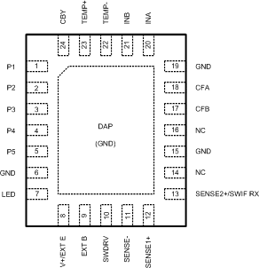
LMP91300 WQFN Terminal Functions
| TERMINAL NUMBER | NAME | TYPE | DESCRIPTION |
|---|---|---|---|
| 1-5 | P1-5 | G | Connect to Ground |
| 6 | GND | G | Board Ground |
| 7 | LED | O | LED Driver Output |
| 8 | V+/EXT E | P | Chip V+/External transistor, emitter |
| 9 | EXT B | P | External transistor, base |
| 10 | SWDRV | O | Drive for external transistor switch |
| 11 | SENSE- | I | Negative sense Input |
| 12 | SENSE1+ | I | Positive sense Input |
| 13 | SENSE2+/SWIF RX | I | Positive sense Input and Single Wire Interface receive |
| 14 | NC | N/A | No connect |
| 15 | GND | G | Board ground |
| 16 | NC | N/A | No connect |
| 17 | CFB | I | Filter capacitor value based on sensor oscillation frequency |
| 18 | CFA | I | Filter capacitor value based on sensor oscillation frequency |
| 19 | GND | G | Board ground |
| 20 | INA | I | External LC tank |
| 21 | INB | I | External LC tank |
| 22 | TEMP- | G | NTC ground, connect to board ground |
| 23 | TEMP+ | I | Analog Temperature Sensor Input |
| 24 | CBY | O | Bypass capacitor (56nF) |
| DAP | DAP | G | Connect to Ground |
LMP91300 DSBGA
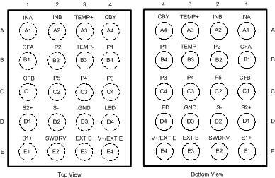
LMP91300 DSBGA Terminal Functions
| TERMINAL NUMBER | NAME | TYPE | DESCRIPTION |
|---|---|---|---|
| A1 | INA | I | External LC tank |
| A2 | INB | I | External LC tank |
| A3 | TEMP+ | I | Analog Temperature Sensor Input |
| A4 | CBY | O | Bypass capacitor (56nF) |
| B1 | CFA | I | Filter capacitor value based on sensor oscillation frequency |
| B2 | P2 | G | Connect to Ground |
| B3 | TEMP- | G | NTC ground, connect to board ground |
| B4 | P1 | G | Connect to Ground |
| C1 | CFB | I | Filter capacitor value based on sensor oscillation frequency |
| C2 | P5 | G | Connect to Ground |
| C3 | P4 | G | Connect to Ground |
| C4 | P3 | G | Connect to Ground |
| D1 | SENSE2+/SWIF RX | I | Positive sense Input and Single Wire Interface receive |
| D2 | SENSE- | I | Negative sense Input |
| D3 | GND | G | Board ground |
| D4 | LED | O | LED Driver Output |
| E1 | SENSE1+ | I | Positive sense Input |
| E2 | SWDRV | O | Drive for external transistor switch |
| E3 | EXT B | P | External transistor, base |
| E4 | V+/EXT E | P | Chip V+/External transistor, emitter |