SNVS814B June   2012  – June 2019 LMR10530

PRODUCTION DATA.  

  1. Features
  2. Applications
  3. Description
    1.     Device Images
      1.      Typical Application
  4. Revision History
  5. Pin Configuration and Functions
    1.     Pin Descriptions
  6. Specifications
    1. 6.1 Absolute Maximum Ratings
    2. 6.2 Recommended Operating Ratings
    3. 6.3 Electrical Characteristics
    4. 6.4 Typical Characteristics
  7. Detailed Description
    1. 7.1 Overview
    2. 7.2 Functional Block Diagram
    3. 7.3 Feature Description
      1. 7.3.1 Frequency Foldback
      2. 7.3.2 Load Step Response
      3. 7.3.3 Output Overvoltage Protection
      4. 7.3.4 Undervoltage Lockout
      5. 7.3.5 Current Limit
      6. 7.3.6 Soft Start/Shutdown
      7. 7.3.7 Thermal Shutdown
  8. Application and Implementation
    1. 8.1 Application Information
    2. 8.2 Typical Application
      1. 8.2.1 Detailed Design Procedure
        1. 8.2.1.1 Custom Design With WEBENCH® Tools
        2. 8.2.1.2 Inductor Selection
        3. 8.2.1.3 Input Capacitor
        4. 8.2.1.4 Output Capacitor
        5. 8.2.1.5 Catch Diode
        6. 8.2.1.6 Output Voltage
        7. 8.2.1.7 Efficiency Estimation
      2. 8.2.2 Application Curve
      3. 8.2.3 Other System Examples
        1. 8.2.3.1 LMR10530X Design Example 1
        2. 8.2.3.2 LMR10530X Design Example 2
        3. 8.2.3.3 LMR10530Y Design Example 3
        4. 8.2.3.4 LMR10530Y Design Example 4
  9. Layout
    1. 9.1 Layout Considerations
  10. 10Device and Documentation Support
    1. 10.1 Device Support
      1. 10.1.1 Third-Party Products Disclaimer
      2. 10.1.2 Development Support
        1. 10.1.2.1 Custom Design With WEBENCH® Tools
    2. 10.2 Receiving Notification of Documentation Updates
    3. 10.3 Community Resources
    4. 10.4 Trademarks
    5. 10.5 Electrostatic Discharge Caution
    6. 10.6 Glossary
  11. 11Mechanical, Packaging, and Orderable Information
  12. 12Mechanical, Packaging, and Orderable Information

Package Options

Mechanical Data (Package|Pins)
Thermal pad, mechanical data (Package|Pins)
Orderable Information

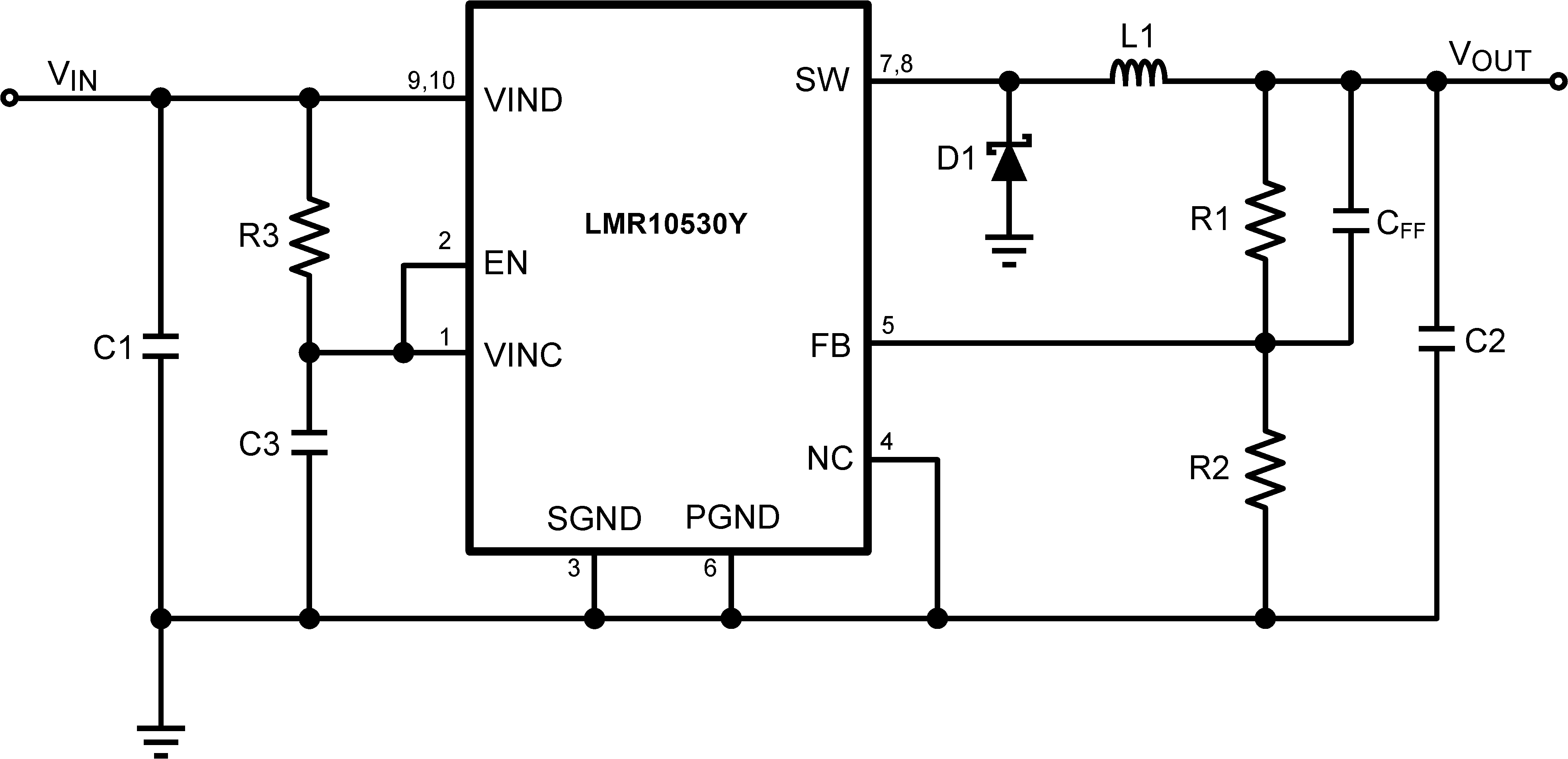
LMR10530Y Design Example 4

LMR10530 30167368.png
VIN = 5 V VOUT = 3.3 V IOUT = 3 A
Figure 35. LMR10530Y (3 MHz)

Table 5. Bill Of Materials

DEVICE ID DEVICE VALUE MANUFACTURER DEVICE NUMBER
U1 3-A buck regulator TI LMR10530Y
C1, Input Capacitor 22 µF, 6.3 V, X5R TDK C3216X5R0J226M
C2, Output Capacitor 47 µF, 6.3 V, X5R TDK C3216X5R0J476M
C3, Bypass Capacitor 0.22 µF, 10 V, X7R Murata GRM216R71A224KC01D
CFF, Feedforward Capacitor 47 nF, 10 V, X7R AVX 0805ZC473JAZ2A
D1, Catch Diode Schottky, 0.43 V at 3 A, VR= 30 V Vishay SSA33L-E3/61T
L1 1 µH, 4 A Taiyo Yuden NP04SZB1R0N
R1 10.2 kΩ, 1% Vishay CRCW080510K2FKEA
R2 2.26 kΩ, 1% Vishay CRCW08052K26FKEA
R3 10 Ω, 1% Vishay CRCW080510R0FKEA