SNVSB99C October 2019 – November 2020 LMR33640
PRODUCTION DATA
- 1 Features
- 2 Applications
- 3 Description
- 4 Revision History
- 5 Device Comparison Table
- 6 Pin Configuration and Functions
- 7 Specifications
- 8 Detailed Description
- 9 Application and Implementation
- 10Power Supply Recommendations
- 11Layout
- 12Device and Documentation Support
- 13Mechanical, Packaging, and Orderable Information
Package Options
Mechanical Data (Package|Pins)
- DDA|8
Thermal pad, mechanical data (Package|Pins)
- DDA|8
Orderable Information
3 Description
The LMR33640 SIMPLE SWITCHER® regulator is an easy-to-use, synchronous, step-down DC/DC converter that delivers best-in-class efficiency for rugged industrial applications. The LMR33640 drives up to 4 A of load current from an input of up to 36 V. The LMR33640 provides high light-load efficiency and output accuracy. Features such as a power-good flag and precision enable provide both flexible and easy-to-use solutions for a wide range of applications. The LMR33640 automatically folds back frequency at light load to improve efficiency. Protection features include thermal shutdown, input undervoltage lockout, cycle-by-cycle current limit, and hiccup short-circuit protection. Integration and internal compensation eliminates many external components and provides a pinout designed for a simple PCB layout. The feature set of the device is designed to simplify implementation for a wide range of end equipment. The LMR33640 is pin-to-pin compatible with the LMR33610, LMR33620, LMR33630 (36 V, 1 A/2, A/3 A), LMR36510 (65 V, 1 A), and LMR36520 (65 V, 2 A), completing the family of scalable SIMPLE SWITCHER power supplies. This minimizes the cost and effort associated with board layout modifications. The LMR33640 is available in an 8-pin HSOIC package.
| PART NUMBER | PACKAGE(1) | BODY SIZE (NOM) |
|---|---|---|
| LMR33640 | HSOIC (8) | 5.00 mm × 4.00 mm |
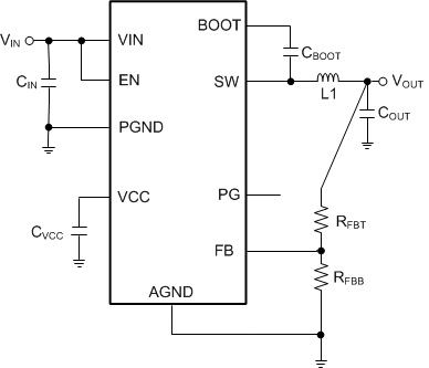
 Simplified Schematic
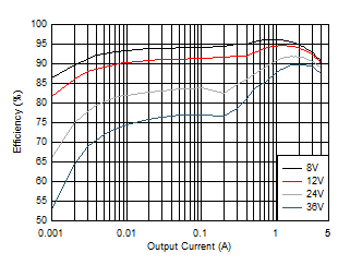
 Efficiency versus Output
Current VOUT = 5 V,
Efficiency versus Output
Current VOUT = 5 V,400 kHz, HSOIC