SNVSBB4B December 2019 – November 2022 LMR36503
PRODUCTION DATA
- 1 Features
- 2 Applications
- 3 Description
- 4 Revision History
- 5 Device Comparison Table
- 6 Pin Configuration and Functions
- 7 Specifications
-
8 Detailed Description
- 8.1 Overview
- 8.2 Functional Block Diagram
- 8.3
Feature Description
- 8.3.1 Enable, Start-up, and Shutdown
- 8.3.2 Adjustable Switching Frequency (with RT)
- 8.3.3 Power-Good Output Operation
- 8.3.4 Internal LDO, VCC UVLO, and VOUT/BIAS Input
- 8.3.5 Bootstrap Voltage and VCBOOT-UVLO (CBOOT Terminal)
- 8.3.6 Output Voltage Selection
- 8.3.7 Soft Start and Recovery from Dropout
- 8.3.8 Current Limit and Short Circuit
- 8.3.9 Thermal Shutdown
- 8.3.10 Input Supply Current
- 8.4 Device Functional Modes
-
9 Application and Implementation
- 9.1 Application Information
- 9.2
Typical Application
- 9.2.1 Design Requirements
- 9.2.2 Detailed Design Procedure
- 9.2.3 Application Curves
- 9.3 Best Design Practices
- 9.4 Power Supply Recommendations
- 9.5 Layout
- 10Device and Documentation Support
- 11Mechanical, Packaging, and Orderable Information
Package Options
Mechanical Data (Package|Pins)
- RPE|9
Thermal pad, mechanical data (Package|Pins)
- RPE|9
Orderable Information
8.3.10 Input Supply Current
The LMR36503 is designed to have very low input supply current when regulating light loads. This is achieved by powering much of the internal circuitry from the output. The VOUT/BIAS pin in the fixed-output voltage variants is the input to the LDO that powers the majority of the control circuits. By connecting the VOUT/BIAS input pin to the output node of the regulator, a small amount of current is drawn from the output. This current is reduced at the input by the ratio of VOUT / VIN.
Equation 3. 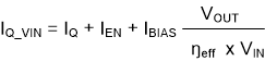
where
- IQ_VIN is the total standby (switching) current consumed by the operating (switching) buck converter when unloaded.
- IQ is the current drawn from the VIN terminal. Check IQ_13p5_Fixed or IQ_24p0_Fixed in Section 7.5 for IQ.
- IEN is current drawn by the EN terminal. Include this current if EN is connected to VIN. Check ILKG-EN in Section 7.5 for IEN.
- IBIAS is bias current drawn by the BIAS input. Check IB_13p5 or IB_24p0 in Section 7.5 for IBIAS.
- ηeff is the light-load efficiency of the buck converter with IQ_VIN removed from the input current of the buck converter. ηeff = 0.8 is a conservative value that can be used under normal operating conditions. This can be traced back as the ISUPPLY in Section 7.7.