SNVS158E March 2001 – December 2016 LMS33460
PRODUCTION DATA.
- 1 Features
- 2 Applications
- 3 Description
- 4 Revision History
- 5 Pin Configuration and Functions
- 6 Specifications
- 7 Detailed Description
- 8 Application and Implementation
- 9 Power Supply Recommendations
- 10Layout
- 11Device and Documentation Support
- 12Mechanical, Packaging, and Orderable Information
Package Options
Mechanical Data (Package|Pins)
- DCK|5
Thermal pad, mechanical data (Package|Pins)
Orderable Information
6 Specifications
6.1 Absolute Maximum Ratings
over operating free-air temperature range (unless otherwise noted)(1)| MIN | MAX | UNIT | |
|---|---|---|---|
| Input voltage to GND | 8 | V | |
| Output voltage to GND | 8 | V | |
| Output continuous output current | 30 | mA | |
| Vapor phase IR convection reflow | 240 | °C | |
| Junction temperature, TJ | 150 | °C | |
| Storage temperature, Tstg | –65 | 150 | °C |
(1) Stresses beyond those listed under Absolute Maximum Ratings may cause permanent damage to the device. These are stress ratings only, which do not imply functional operation of the device at these or any other conditions beyond those indicated under Recommended Operating Conditions. Exposure to absolute-maximum-rated conditions for extended periods may affect device reliability.
6.2 ESD Ratings
| VALUE | UNIT | |||
|---|---|---|---|---|
| V(ESD) | Electrostatic discharge | Human-body model (HBM), per ANSI/ESDA/JEDEC JS-001(1) | ±2500 | V |
| Machine model | ±200 | |||
(1) JEDEC document JEP155 states that 500-V HBM allows safe manufacturing with a standard ESD control process.
6.3 Recommended Operating Conditions
| MIN | MAX | UNIT | ||
|---|---|---|---|---|
| TJ | Operating junction temperature | –40 | 85 | °C |
6.4 Thermal Information
| THERMAL METRIC(1) | LMS33460 | UNIT | |
|---|---|---|---|
| DCK (SC70) | |||
| 5 PINS | |||
| RθJA | Junction-to-ambient thermal resistance | 275.5 | °C/W |
| RθJC(top) | Junction-to-case (top) thermal resistance | 102.5 | °C/W |
| RθJB | Junction-to-board thermal resistance | 54 | °C/W |
| ψJT | Junction-to-top characterization parameter | 2.7 | °C/W |
| ψJB | Junction-to-board characterization parameter | 53.3 | °C/W |
(1) For more information about traditional and new thermal metrics, see the Semiconductor and IC Package Thermal Metrics application report.
6.5 Electrical Characteristics
TJ = 25°C (unless otherwise noted)| PARAMETER | TEST CONDITIONS | MIN | TYP | MAX | UNIT | |
|---|---|---|---|---|---|---|
| VDET | Detector threshold | VIN falling | 2.85 | 3 | 3.15 | V |
| VHYS | Detector voltage hysteresis | VIN rising | 0.095 | 0.155 | 0.215 | V |
| IIN | Input supply current | VIN = 2.87 V | 1 | 2.2 | µA | |
| VIN = 4.7 V | 1.2 | 3.6 | µA | |||
| VIN = 7 V(1) | 25 | 200 | µA | |||
| VIN(MAX) | Maximum operating voltage | 7 | V | |||
| VIN(MIN) | Minimum operating voltage | 0.7 | 1.1 | V | ||
| TJ = –40°C to 85°C | 1 | 1.3 | ||||
| IOUT(LOW) | Output current low | VOUT = 0.05 V, VIN = 1.1 V | 0.01 | 0.6 | mA | |
| VOUT = 0.5 V, VIN = 1.5 V | 2 | 11 | ||||
| tPDHL | Output delay time (output transition high to low ) | CL = 10 pF, RL = 470 kΩ | 130 | 200 | µs | |
| ΔVDET/ΔT | Detect voltage temperature coefficient | TJ = –40°C to 85°C | ±120 | PPM/°C | ||
(1) Quiescent current increases substantially above 5.5 V, but is very low in the normal range below 5.5 V.
6.6 Typical Characteristics
TA = 25°C, RL = 470 kΩ, and CL = 10 pF (unless otherwise noted)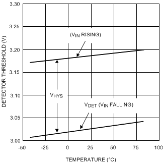 Figure 1. Detector Threshold vs Temperature
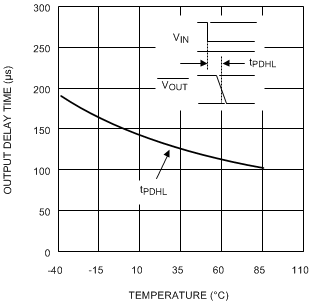 Figure 3. Propagation Delay Time (tPDHL) vs Temperature
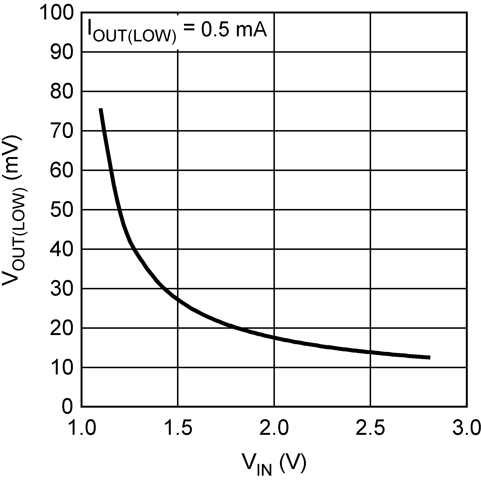 Figure 5. VOUT(LOW) vs VIN
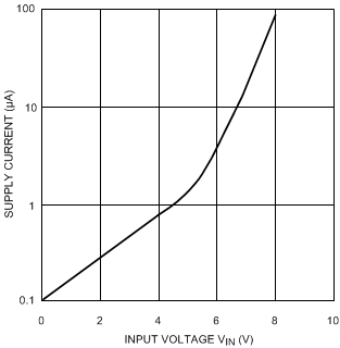 Figure 2. Supply Current vs Input Voltage
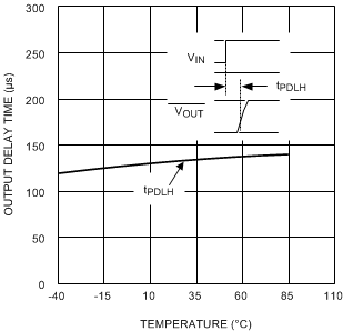 Figure 4. Propagation Delay Time (tPDLH) vs Temperature