SNOS018H August 1999 – December 2014 LMV331-N , LMV339-N , LMV393-N
PRODUCTION DATA.
- 1 Features
- 2 Applications
- 3 Description
- 4 Revision History
- 5 Pin Configuration and Functions
- 6 Specifications
- 7 Detailed Description
- 8 Application and Implementation
- 9 Power Supply Recommendations
- 10Layout
- 11Device and Documentation Support
- 12Mechanical, Packaging, and Orderable Information
Package Options
Mechanical Data (Package|Pins)
Thermal pad, mechanical data (Package|Pins)
Orderable Information
10 Layout
10.1 Layout Guidelines
Comparators are very sensitive to input noise. For best results, the following layout guidelines should be maintained:
- Use a printed circuit board (PCB) with a good, unbroken low-inductance ground plane. Proper grounding (use of ground plane) helps maintain specified performance of the comparator
- Connect low-ESR, 0.1-μF ceramic bypass capacitors between each supply pin and ground, placed as close to the device as possible. A single bypass capacitor from V+ to ground is applicable for single supply applications.
- Separate grounding for analog and digital portions of circuitry is one of the simplest and most-effective methods of noise suppression. One or more layers on multilayer PCBs are usually devoted to ground planes. A ground plane helps distribute heat and reduces EMI noise pickup. Make sure to physically separate digital and analog grounds paying attention to the flow of the ground current. For more detailed information refer to SLOA089, Circuit Board Layout Techniques.
- In order to reduce parasitic coupling, run the input traces as far away from the supply or output traces as possible. If it is not possible to keep them separate, it is much better to cross the sensitive trace perpendicular as opposed to in parallel with the noisy trace.
- Place the external components as close to the device as possible, as shown in Layout Example.
- Keep the length of input traces as short as possible. Always remember that the input traces are the most sensitive part of the circuit.
- For slow-moving input signals, take care to prevent parasitic feedback. A small capacitor (1000 pF or less) placed between the inputs can help eliminate oscillations in the transition region. This capacitor causes some degradation to propagation delay when the impedance is low. Run the topside ground plane between the output and inputs.
10.2 Layout Example
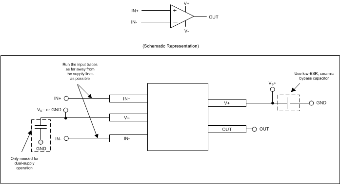 Figure 27. Comparator Board Layout