SLOS263Y august 1999 – august 2023 LMV321 , LMV324 , LMV358
PRODUCTION DATA
- 1
- 1 Features
- 2 Applications
- 3 Description
- 4 Revision History
- 5 Pin Configuration and Functions
- 6 Specifications
- 7 Detailed Description
- 8 Application and Implementation
- 9 Device and Documentation Support
- 10Mechanical, Packaging, and Orderable Information
Package Options
Refer to the PDF data sheet for device specific package drawings
Mechanical Data (Package|Pins)
- D|8
- DGK|8
- PW|8
Thermal pad, mechanical data (Package|Pins)
Orderable Information
8.1.2 Detailed Design Procedure
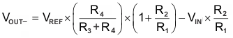
The circuit in Figure 8-1 takes a single-ended input signal, VIN, and generates two output signals, VOUT+ and VOUT– using two amplifiers and a reference voltage, VREF. VOUT+ is the output of the first amplifier and is a buffered version of the input signal, VIN (see Equation 1). VOUT– is the output of the second amplifier which uses VREF to add an offset voltage to VIN and feedback to add inverting gain. The transfer function for VOUT– is Equation 2.
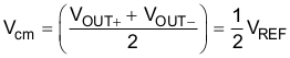
The differential output signal, VDIFF, is the difference between the two single-ended output signals, VOUT+ and VOUT–. Equation 3 shows the transfer function for VDIFF. By applying the conditions that R1 = R2 and R3 = R4, the transfer function is simplified into Equation 6. Using this configuration, the maximum input signal is equal to the reference voltage and the maximum output of each amplifier is equal to the VREF. The differential output range is 2×VREF. Furthermore, the common mode voltage will be one half of VREF (see Equation 7).