SNVS708G March 2011 – August 2015 LMZ23608
PRODUCTION DATA.
- 1 Features
- 2 Applications
- 3 Description
- 4 Revision History
- 5 Pin Configuration and Functions
- 6 Specifications
- 7 Detailed Description
-
8 Application and Implementation
- 8.1 Application Information
- 8.2
Typical Application
- 8.2.1 Design Requirements
- 8.2.2
Detailed Design Procedure
- 8.2.2.1 Design Steps
- 8.2.2.2 Enable Divider, RENT, RENB and RENH Selection
- 8.2.2.3 Output Voltage Selection
- 8.2.2.4 Soft-Start Capacitor Selection
- 8.2.2.5 Tracking Supply Divider Option
- 8.2.2.6 COUT Selection
- 8.2.2.7 CIN Selection
- 8.2.2.8 Discontinuous Conduction and Continuous Conduction Modes Selection
- 8.2.3 Application Curves
- 9 Power Supply Recommendations
- 10Layout
- 11Device and Documentation Support
- 12Mechanical, Packaging, and Orderable Information
Package Options
Mechanical Data (Package|Pins)
- NDY|11
Thermal pad, mechanical data (Package|Pins)
Orderable Information
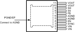
5 Pin Configuration and Functions
NDY Package
11-Pin
Top View

Pin Functions
| PIN | I/O | DESCRIPTION | |
|---|---|---|---|
| NAME | NO. | ||
| AGND | 5 | Ground | Analog Ground — Reference point for all stated voltages. Must be externally connected to EP/PGND. |
| 6 | |||
| EN | 4 | Analog | Enable — Input to the precision enable comparator. Rising threshold is 1.274 V typical. Once the module is enabled, a 20-µA source current is internally activated to accommodate programmable hysteresis. |
| FB | 7 | Analog | Feedback — Internally connected to the regulation, overvoltage, and short circuit comparators. The regulation reference point is 0.8 V at this input pin. Connect the feedback resistor divider between the output and AGND to set the output voltage. |
| PGND | — | Ground | Exposed Pad / Power Ground Electrical path for the power circuits within the module. — NOT Internally connected to AGND / pin 5. Used to dissipate heat from the package during operation. Must be electrically connected to pin 5 external to the package. |
| SH | 9 | Analog | Share pin. Connect this to the share pin of other LMZ23608 modules to share the load between the devices. One device must be configured as the master by connecting the FB normally. All other devices must be configured as slaves by leaving their respective FB pins floating. Leave this pin floating if not used, do not ground. See Design Steps section. |
| SS | 8 | Analog | Soft-Start/Track input — To extend the 1.6-ms internal soft-start connect an external soft-start capacitor. For tracking connect to an external resistive divider connected to a higher priority supply rail. See Design Steps section. |
| SYNC | 3 | Analog | Sync Input — Apply a CMOS logic level square wave whose frequency is between 350 kHz and 600 kHz to synchronize the PWM operating frequency to an external frequency source. When not using synchronization this pin must be tied to ground. The module free running PWM frequency is 350 kHz. |
| VOUT | 10 | Power | Output Voltage — Output from the internal inductor. Connect the output capacitor between this pin and PGND. |
| 11 | |||
| VIN | 1 | Power | Supply input — Nominal operating range is 6 V to 36 V. A small amount of internal capacitance is contained within the package assembly. Additional external input capacitance is required between this pin and PGND. |
| 2 | |||