SNOSA40K November 2002 – December 2016 LP2996-N , LP2996A
PRODUCTION DATA.
- 1 Features
- 2 Applications
- 3 Description
- 4 Revision History
- 5 Pin Configuration and Functions
- 6 Specifications
- 7 Detailed Description
- 8 Applications and Implementation
- 9 Power Supply Recommendations
- 10Layout
- 11Device and Documentation Support
- 12Mechanical, Packaging, and Orderable Information
Package Options
Mechanical Data (Package|Pins)
Thermal pad, mechanical data (Package|Pins)
- DDA|8
Orderable Information
7 Detailed Description
7.1 Overview
The LP2996-N and LP2996A devices can be used to provide a termination voltage for additional logic schemes such as SSTL-3 or HSTL.
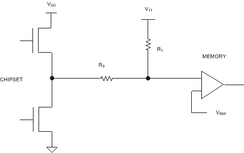
Series Stub Termination Logic (SSTL) was created to improve signal integrity of the data transmission across the memory bus. This termination scheme is essential to prevent data error from signal reflections while transmitting at high frequencies encountered with DDR-SDRAM. The most common form of termination is Class II single parallel termination. This involves one RS series resistor from the chipset to the memory and one RT termination resistor. Typical values for RS and RT are 25 Ω, although these can be changed to scale the current requirements from the LP2996-N or LP2996A. This implementation is shown in Figure 17.
 Figure 17. SSTL-Termination Scheme
7.2 Functional Block Diagram

7.3 Feature Description
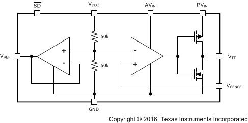
The LP2996-N and LP2996A are linear bus termination regulators designed to meet the JEDEC requirements of SSTL-2. The output (VTT) is capable of sinking and sourcing current while regulating the output voltage equal to VDDQ / 2. The output stage is designed to maintain excellent load regulation while preventing shoot through. The LP2996-N and LP2996A also incorporate two distinct power rails that separates the analog circuitry from the power output stage. This allows a split rail approach to be used to decrease internal power dissipation. It also permits the LP2996-N to provide a termination solution for DDR2-SDRAM, while the LP2996A supports DDR3-SDRAM and DDR3L-SDRAM memory. TI recommends the LP2998 and LP2998-Q1 for all DDR applications that require operation at below-zero temperatures.
7.4 Device Functional Modes
7.4.1 Start-Up
During start up when VDDQ is enabled, the error amplifier senses the output voltage is low and drives the pass element hard causing a large inrush current. If this inrush current is too large, the device shuts down and restarts due to the internal current limit. Two solutions to prevent large inrush current during start up:
- Slow down the slew rate of VDDQ. When the slew rate of VDDQ is fast (approximately 60 µs), the input current can reach over 5 A which exceeds the device’s current limit thus causing a restart. If VDDQ start-up slew rate is ≥300 µs, the inrush current can be reduced by 90% limiting the input rush current to less than 500mA.
- In some cases the system designers have very little to no control over the VDDQ voltage supply slew rate, whether using linear or switching regulators. Some step down voltage regulators do not have soft-start feature. VDDQ voltage source requires only 18 µA current to enable the DDRII termination voltage. Therefore placing an RC filter at VDDQ pin can conveniently increase the output voltage slew rate, allowing a slow rise in capacitor charge current. To keep the VDDQ voltage losses minimum, the resistor value must be chosen carefully. Using a 100-Ω resistor keeps the VDDQ supply voltage losses down to 1.8 mV, because the current through VDDQ is only 18 µA for DDRIII configuration.
See Limiting DDR Termination Regulators’ Inrush Current (SNVA758) for more information relating to the inrush current during start up.
7.4.2 Normal Operation
The device contains a high-speed operational amplifier to provide excellent response to load transients. The output stage prevents shoot through while delivering 1.5-A continuous current and transient peaks up to 3 A in the application as required for DDR-SDRAM termination. The LP2996-N and LP2996A also incorporate a VSENSE pin to provide superior load regulation and a VREF output as a reference for the chipset and DIMMs. See Electrical Characteristics and Application Information.
7.4.3 Shutdown
The LP2996-N and LP2996A feature an active-low shutdown (SD) pin that provides Suspend To RAM (STR) functionality. When SD is pulled low, the VTT output tri-states providing a high impedance output, but VREF remains active. A power savings advantage can be obtained in this mode through lower quiescent current. During shutdown, VTT must not be exposed to voltages that exceed AVIN. With the shutdown pin asserted low the quiescent current of the LP2996-N and LP2996A drops, however, VDDQ always maintains its constant impedance of 100 kΩ for generating the internal reference. Therefore, to calculate the total power loss in shutdown, both currents must be considered. The shutdown pin also has an internal pullup current, therefore to turn the part on, the shutdown pin can either be connected to AVIN or left open.