SNVS003G June 1999 – April 2016 LP3470
PRODUCTION DATA.
- 1 Features
- 2 Applications
- 3 Description
- 4 Revision History
- 5 Pin Configuration and Functions
- 6 Specifications
- 7 Detailed Description
- 8 Application and Implementation
- 9 Power Supply Recommendations
- 10Layout
- 11Device and Documentation Support
- 12Mechanical, Packaging, and Orderable Information
Package Options
Mechanical Data (Package|Pins)
- DBV|5
Thermal pad, mechanical data (Package|Pins)
Orderable Information
7 Detailed Description
Overview
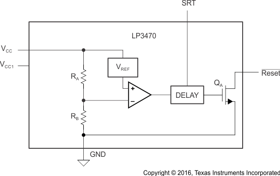
The LP3470 micropower voltage supervisory circuit provides a simple solution to monitor the power supplies in microprocessor and digital systems and provides a reset controlled by the factory-programmed reset threshold on the VCC supply voltage pin. When the voltage declines below the reset threshold, the reset signal is asserted and remains asserted for an interval programmed by an external capacitor after VCC has risen above the threshold voltage. The reset threshold options are 2.63 V, 2.93 V, 3.08 V, 3.65 V, 4 V, 4.38 V, 4.63 V.
7.1 Functional Block Diagram

7.2 Feature Description
7.2.1 Reset Time-Out Period
The reset time-out period (tRP) is programmable using an external capacitor (C1) connected to pin SRT of LP3470. A ceramic chip capacitor rated at or above 10 V is sufficient. The reset time-out period (tRP) can be calculated using Equation 1.
For example a C1 of 100 nF will achieve a tRP of 200 ms. If no delay due to tRP is needed in a certain application, the pin SRT must be left floating.
7.2.2 Reset Output
In applications like microprocessor (µP) systems, errors might occur in system operation during power up, power down, or brownout conditions. It is imperative to monitor the power supply voltage to prevent these errors from occurring.
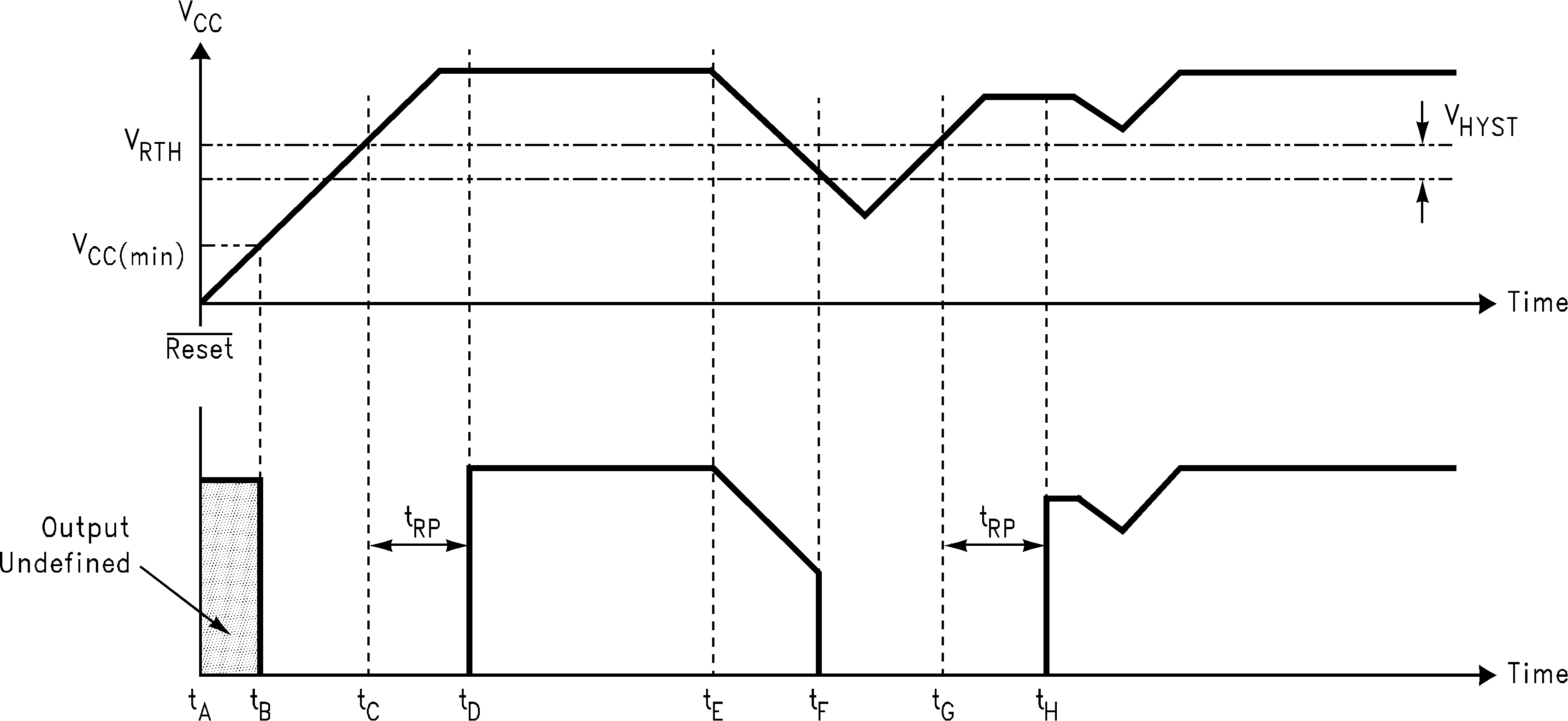
The LP3470 asserts a reset signal whenever the VCC supply voltage is below a threshold (VRTH) voltage. Reset is ensured to be a logic low for VCC > 0.5 V. Once VCC exceeds the reset threshold, the reset is kept asserted for a time period (tRP) programmed by an external capacitor (C1); after this interval Reset goes to logic high. If a brownout condition occurs (monitored voltage falls below the reset threshold minus a small hysteresis), Reset goes low. When VCC returns above the reset threshold, Reset remains low for a time period tRP before going to logic high. Figure 9 shows this behavior.
 Figure 9. Reset Output Timing Diagram
7.2.3 Pullup Resistor Selection
The Reset output structure of the LP3470 is a simple open-drain N-channel MOSFET switch. A pullup resistor (R1) must be connected to VCC.
R1 must be large enough to limit the current through the output MOSFET (Q1) below 10 mA. A resistor value of more than 680 Ω ensures this. R1 must also be small enough to ensure a logic high while supplying all the leakage current through the Reset pin. A resistor value of less than 68 kΩ satisfies this condition. A typical pullup resistor value of 20 kΩ is sufficient in most applications.
7.2.4 Negative-Going VCC Transients
The LP3470 is relatively immune to short duration negative-going VCC transients (glitches). The Typical Characteristics show the maximum transient duration versus negative transient amplitude (see Figure 6), for which reset pulses are not generated. This graph shows the maximum pulse width a negative-going VCC transient may typically have without causing a reset pulse to be issued. As the transient amplitude increases (in other words, goes farther below the reset threshold), the maximum allowable pulse width decreases. A 0.1-µF bypass capacitor mounted close to VCC provides additional transient immunity.
7.3 Device Functional Modes
7.3.1 Reset Output Low
When the VCC supply voltage is below a threshold (VRTH) voltage minus a hysteresis (VHYST) voltage, the Reset pin will output logic low. Reset is ensured to be a logic low for VCC > 0.5 V.
7.3.2 Reset Output High
When the VCC supply voltage exceeds the reset threshold, the Reset is kept asserted for a time period (tRP) programmed by an external capacitor (C1); after this interval Reset goes to logic high.