SNVS247E September 2003 – August 2016 LP3875-ADJ
PRODUCTION DATA.
- 1 Features
- 2 Applications
- 3 Description
- 4 Revision History
- 5 Pin Configuration and Functions
- 6 Specifications
- 7 Detailed Description
-
8 Application and Implementation
- 8.1 Application Information
- 8.2
Typical Application
- 8.2.1 Design Requirements
- 8.2.2
Detailed Design Procedure
- 8.2.2.1 External Capacitors
- 8.2.2.2 CFF (Feed Forward Capacitor)
- 8.2.2.3 Selecting a Capacitor
- 8.2.2.4 Capacitor Characteristics
- 8.2.2.5 Setting The Output Voltage
- 8.2.2.6 Turnon Characteristics for Output Voltages Programmed to 2 V or Less
- 8.2.2.7 RFI/EMI Susceptibility
- 8.2.2.8 Output Noise
- 8.2.2.9 Power Dissipation
- 8.2.2.10 Estimating Junction Temperature
- 8.2.3 Application Curves
- 9 Power Supply Recommendations
- 10Layout
- 11Device and Documentation Support
- 12Mechanical, Packaging, and Orderable Information
Package Options
Mechanical Data (Package|Pins)
Thermal pad, mechanical data (Package|Pins)
- KTT|5
Orderable Information
7 Detailed Description
7.1 Overview
The LP3875-ADJ linear regulators is designed to provide an ultra-low-dropout voltage with excellent transient response and load/line regulation. For battery-powered always-on type applications, the very low quiescent current of the LP3875-ADJ in shutdown mode helps reduce battery drain.
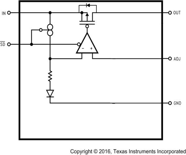
7.2 Functional Block Diagram

7.3 Feature Description
7.3.1 Shutdown (SD)
The LM3875-ADJ device has a shutdown feature that turns the device off and reduces the quiescent current to 10 nA (typical).
7.3.2 Short-Circuit Protection
The LP3875-ADJ is short-circuit protected and, in the event of a peak overcurrent condition, the short-circuit control loop rapidly drives the output PMOS pass element off. Once the power pass element shuts down, the control loop rapidly cycles the output on and off until the average power dissipation causes the thermal shutdown circuit to respond to servo the on/off cycling to a lower frequency. Refer to Power Dissipation for power dissipation calculations.
7.3.3 Dropout Voltage
The dropout voltage of a regulator is defined as the minimum input-to-output differential required to stay within 2% of the nominal output voltage. For CMOS LDOs, the dropout voltage is the product of the load current and the RDS(ON) of the internal MOSFET.
7.4 Device Functional Modes
7.4.1 Shutdown Mode
A CMOS logic low level signal at the shutdown (SD) pin turns off the regulator. The SD pin must be actively terminated through a 10-kΩ pullup resistor for a proper operation. If this pin is driven from a source that actively pulls high and low (such as a CMOS rail-to-rail comparator), the pullup resistor is not required. This pin must be tied to VIN if not used.
7.4.2 Active Mode
When voltage at SD pin of the LP3875-ADJ device is at logic high level, the device is in normal mode of operation.