SNVS185F February 2002 – April 2017 LP3982
PRODUCTION DATA.
- 1 Features
- 2 Applications
- 3 Description
- 4 Revision History
- 5 Pin Configuration and Functions
- 6 Specifications
- 7 Detailed Description
- 8 Application and Implementation
- 9 Power Supply Recommendations
- 10Layout
- 11Device and Documentation Support
- 12Mechanical, Packaging, and Orderable Information
Package Options
Mechanical Data (Package|Pins)
Thermal pad, mechanical data (Package|Pins)
Orderable Information
7 Detailed Description
7.1 Overview
The LP3982 is package, pin, and performance compatible with Maxim's MAX8860, excluding reverse battery protection and dual-mode function (fixed and adjustable combined).
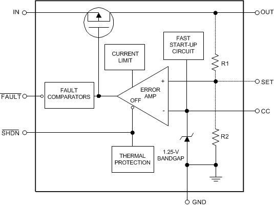
A 1.25-V bandgap reference, an error amplifier, and a PMOS pass transistor perform voltage regulation while being supported by shutdown, fault, and the usual temperature and current protection circuitry (see Functional Block Diagram).
The regulator topology is the classic type with negative feedback from the output to one of the inputs of the error amplifier. Feedback resistors R1 and R2 are either internal or external to the device, depending on whether it is the fixed-voltage version or the adjustable version. The negative feedback and high open loop gain of the error amplifier cause the two inputs of the error amplifier to be virtually equal in voltage. If the output voltage changes due to load changes, the error amplifier provides the appropriate drive to the pass transistor to maintain the error amplifier's inputs as virtually equal. In short, the error amplifier keeps the output voltage constant in order to keep its inputs equal.
7.2 Functional Block Diagram

7.3 Feature Description
7.3.1 No-Load Stability
The LP3982 remains stable during no-load conditions, a necessary feature for CMOS RAM keep-alive applications.
7.4 Device Functional Modes
7.4.1 Shutdown
The LP3982 goes into sleep mode when the SHDN pin is in a logic low condition. During this condition, the pass transistor, error amplifier, and bandgap are turned off, reducing the supply current to 1 nA typical. The maximum voltage for a logic low at the SHDN pin is 0.4 V. A minimum voltage of 2 V at the SHDN pin turns the LP3982 back on. The SHDN pin may be directly tied to VIN to keep the part on. The SHDN pin may exceed VIN but not the maximum of 6.5 V.
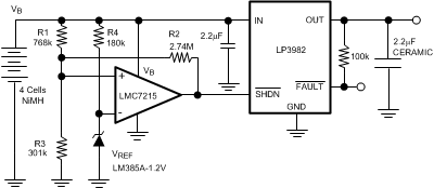
Figure 13 shows an application that uses the SHDN pin. It detects when the battery is too low and disconnects the load by turning off the regulator. A micropower comparator (LMC7215) and reference (LM385) are combined with resistors to set the minimum battery voltage. At the minimum battery voltage, the comparator output goes low and tuns off the LP3982 and corresponding load. Hysteresis is added to the minimum battery threshold to prevent the battery's recovery voltage from falsely indicating an above minimum condition. When the load is disconnected from the battery, it automatically increases in terminal voltage because of the reduced IR drop across its internal resistance. The minimum battery detector of Figure 13 has a low detection threshold (VLT) of 3.6 V that corresponds to the minimum battery voltage. The upper threshold (VUT) is set for 4.6 V to exceed the recovery voltage of the battery.
 Figure 13. Minimum Battery Detector that Disconnects the Load Via the SHDN Pin of the LP3982
Resistor value for VUT and VLT are determined as follows:

(The application of Figure 13 used a GT of 5 μ mho.)


The above procedure assumes a rail-to-rail output comparator. Essentially, R2 is in parallel with R1 prior to reaching the lower threshold, then R2 becomes parallel with R3 for the upper threshold. Note that the application requires rail-to-rail input as well.
The resistor values shown in Figure 13 are the closest practical to calculated values.