SNVS345G June 2006 – December 2014 LP5951
PRODUCTION DATA.
- 1 Features
- 2 Applications
- 3 Description
- 4 Revision History
- 5 Pin Configuration and Functions
- 6 Specifications
- 7 Detailed Description
- 8 Application and Implementation
- 9 Power Supply Recommendations
- 10Layout
- 11Device and Documentation Support
- 12Mechanical, Packaging, and Orderable Information
Package Options
Mechanical Data (Package|Pins)
Thermal pad, mechanical data (Package|Pins)
Orderable Information
6 Specifications
6.1 Absolute Maximum Ratings
over operating free-air temperature (unless otherwise noted)(1)| MIN | MAX | UNIT | ||
|---|---|---|---|---|
| IN pin: Voltage to GND | –0.3 | 6.5 | V | |
| EN pin: Voltage to GND | –0.3 to (VIN + 0.3 V)(2) | 6.5 | ||
| Continuous power dissipation(3) | Internally limited | |||
| Junction temperature (TJ-MAX ) | 150 | °C | ||
| Package peak reflow temperature (10-20 s) | 240 | |||
| Package peak reflow temperature (Pb-free, 10-20 s) | 260 | |||
| Storage temperature, Tstg | –65 | 150 | °C | |
(1) Stresses beyond those listed under Absolute Maximum Ratings may cause permanent damage to the device. These are stress ratings only, which do not imply functional operation of the device at these or any other conditions beyond those indicated under Recommended Operating Conditions. Exposure to absolute-maximum-rated conditions for extended periods may affect device reliability.
(2) The lower of VIN + 0.3 or 6.5 V.
(3) Internal thermal shutdown circuitry protects the device from permanent damage. Thermal shutdown engages at TJ = 160°C (typ.) and disengages at TJ = 140°C (typ.).
6.2 ESD Ratings
| VALUE | UNIT | |||
|---|---|---|---|---|
| V(ESD) | Electrostatic discharge | Human-body model (HBM), per ANSI/ESDA/JEDEC JS-001(1) | ±2000 | V |
(1) JEDEC document JEP155 states that 500-V HBM allows safe manufacturing with a standard ESD control process.
6.3 Recommended Operating Conditions
over operating free-air temperature range (unless otherwise noted)(1)(2)| MIN | NOM | MAX | UNIT | |||
|---|---|---|---|---|---|---|
| VIN | Input voltage | 1.8 | 5.5 | V | ||
| VEN | Enable input voltage | 0 | (VIN + 0.3) | V | ||
| TJ | Junction temperature | –40 | 125 | °C | ||
| TA | Ambient temperature | See Power Dissipation And Device Operation | ||||
(1) Stresses beyond those listed under Absolute Maximum Ratings may cause permanent damage to the device. These are stress ratings only, which do not imply functional operation of the device at these or any other conditions beyond those indicated under Recommended Operating Conditions. Exposure to absolute-maximum-rated conditions for extended periods may affect device reliability.
(2) All voltages are with respect to the potential at the GND pin.
6.4 Thermal Information
| THERMAL METRIC(1) | LP5951 | UNIT | ||
|---|---|---|---|---|
| SOT-23 (DBV) | SC70 (DCK) | |||
| 5 PINS | 5 PINS | |||
| RθJA | Junction-to-ambient thermal resistance | 195.6 | 276.7 | °C/W |
| RθJC(top) | Junction-to-case (top) thermal resistance | 108.3 | 86.3 | |
| RθJB | Junction-to-board thermal resistance | 52.1 | 56.9 | |
| ψJT | Junction-to-top characterization parameter | 11.0 | 1.3 | |
| ψJB | Junction-to-board characterization parameter | 51.6 | 56.1 | |
(1) For more information about traditional and new thermal metrics, see the IC Package Thermal Metrics application report, SPRA953.
6.5 Electrical Characteristics
All typical (TYP) values and limits are for TA = TJ = 25°C, and minimum (MIN) and maximum (MAX) limits apply over the operating junction temperature range (TJ ) of –40°C to 125°C unless otherwise specified in the Test Conditions. Unless otherwise noted, VIN = VOUT(NOM) + 1 V, CIN = 1 µF, COUT = 1 µF, VEN = 0.9 V. (1)(2)| PARAMETER | TEST CONDITIONS | MIN | TYP | MAX | UNIT | |
|---|---|---|---|---|---|---|
| VIN | Input voltage | VIN ≥ VOUT(NOM) + VDO | 1.8 | 5.5 | V | |
| ΔVOUT | Output voltage tolerance | IOUT = 1mA TJ = 25°C |
–2% | 2% | ||
| IOUT = 1mA –30°C ≤ TJ ≤ +125°C |
–3.5% | 3.5% | ||||
| Line regulation error | VIN = VOUT(NOM) + 1 V to 5.5 V IOUT = 1 mA |
0.1 | %/V | |||
| Load regulation error | IOUT = 1 mA to 150 mA | –0.01 | %/mA | |||
| VDO | Output voltage dropout(3) | IOUT = 150 mA , VOUT ≥ 2.5 V | 250 | mV | ||
| IOUT = 150 mA , VOUT < 2.5 V | 200 | 350 | ||||
| IQ | Quiescent current | VEN = 0.9 V, ILOAD = 0 | 29 | 55 | µA | |
| VEN = 0.9 V, ILOAD = 150 mA | 33 | 70 | ||||
| VEN = 0 V, TJ = 25°C | 0.005 | 1 | ||||
| ISC | Output current (short circuit) | VIN = VOUT(NOM) + 1 V | 150 | 400 | mA | |
| PSRR | Power supply rejection ratio | Sine modulated VIN, ƒ = 100 Hz | 60 | dB | ||
| Sine modulated VIN, ƒ = 1 kHz | 60 | |||||
| Sine modulated VIN, ƒ = 10 kHz | 50 | |||||
| EN | Output noise | BW = 10 Hz - 100 kHz | 125 | µVRMS | ||
| TSD | Thermal shutdown | 160 | °C | |||
| Temperature hysteresis | 20 | |||||
(1) All voltages are with respect to the potential at the GND pin.
(2) Minimum and Maximum limits are ensured through test, design, or statistical correlation over the operating junction temperature range (TJ ) of –40°C to 125°C, unless otherwise stated. Typical values represent the most likely parametric norm at TJ = 25°C, and are provided for reference purposes only.
(3) Dropout voltage is defined as the input to output voltage differential at which the output voltage falls to 100 mV below the nominal output voltage. This specification does not apply for output voltages below 1.8 V.
6.6 Enable Control Characteristics
| PARAMETER | TEST CONDITIONS | MIN | TYP | MAX | UNIT | |
|---|---|---|---|---|---|---|
| IEN | Maximum input current at EN input | 0 V ≤ VEN ≤ VIN, VIN = 5.5 V –40°C ≤ TJ ≤ 125°C |
–1 | 1 | µA | |
| VIL | Low input threshold (shutdown) | VIN = 1.8 V to 5.5 V –40°C ≤ TJ ≤ 125°C |
0.4 | V | ||
| VIH | High input threshold (enable) | VIN = 1.8 V to 5.5 V –40°C ≤ TJ ≤ 125°C |
0.9 | |||
6.7 Transient Characteristics
| PARAMETER | TEST CONDITIONS | MIN | TYP | MAX | UNIT | |
|---|---|---|---|---|---|---|
| ΔVOUT | Dynamic line transient | VIN = VOUT(NOM) + 1 V to VOUT(NOM) + 1 V + 0.6 V in 30 µs, no load |
±2 | mV | ||
| ΔVOUT | Dynamic load transient | IOUT = 0 mA to 150 mA in 10 µs IOUT = 150 mA to 0 mA in 10 µs IOUT = 1 mA to 150 mA in 1 µs IOUT = 150 mA to 1 mA in 1 µs |
-30 20 -50 40 |
mV mV mV mV |
||
| ΔVOUT | Overshoot on start-up | Nominal conditions | 10 | mV | ||
| TON | Turnon time | IOUT = 1 mA | 30 | µs | ||
6.8 Output Capacitor, Recommended Specification
| PARAMETER | TEST CONDITIONS | MIN(1) | TYP | MAX(1) | UNIT | |
|---|---|---|---|---|---|---|
| COUT | Output capacitance | Capacitance(2)
IOUT = 150 mA, VIN = 5 V |
0.7 | 1 | 47 | µF |
| ESR | 0.003 | 0.300 | Ω | |||
(1) Min and Max limits are ensured by design.
(2) The capacitor tolerance should be 30% or better over temperature. The full operating conditions for the application should be considered when selecting a suitable capacitor to ensure that the minimum value of capacitance is always met. Recommended capacitor type is X7R. However, dependent on application, X5R, Y5V, and Z5U can also be used. The shown minimum limit represents real minimum capacitance, including all tolerances and must be maintained over temperature and dc bias voltage (see External Capacitors in Application and Implementation section).
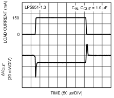
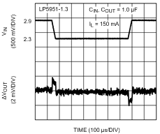
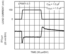
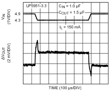
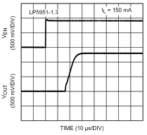
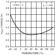
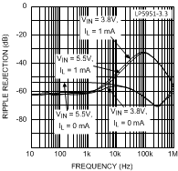
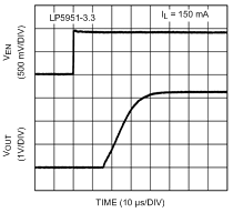
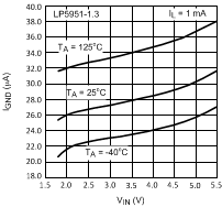
6.9 Typical Characteristics
Unless otherwise specified, CIN = 1 µF ceramic, COUT = 1 µF ceramic, VIN = VOUT(NOM) + 1 V, TA = 25°C; EN pin is tied to VIN.