SNVS857 February 2014 LP8555
PRODUCTION DATA.
- 1 Features
- 2 Applications
- 3 Description
- 4 Simplified Schematic
- 5 Revision History
- 6 Terminal Configuration and Functions
- 7 Specifications
-
8 Detailed Description
- 8.1 Overview
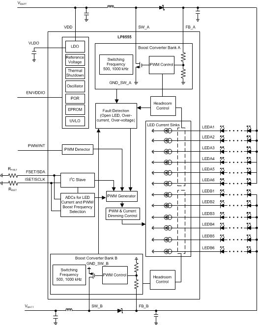
- 8.2 Functional Block Diagram
- 8.3
Features Description
- 8.3.1 Boost Converter Overview
- 8.3.2 Brightness Control
- 8.3.3 LED Brightness Slopes, Normal and Advanced
- 8.3.4
Start-up and Shutdown Sequences
- 8.3.4.1 Start-up With PWM Input Brightness Control Mode (BRTMODE = 00b)
- 8.3.4.2 Shutdown With PWM Input Brightness Control Mode (BRTMODE = 00b)
- 8.3.4.3 Start-up With I2C Brightness Control Mode (BRTMODE = 01b)
- 8.3.4.4 Shutdown With I2C Brightness Control Mode (BRTMODE = 01b)
- 8.3.4.5 Start-up with I2C + PWM Input Brightness Control Mode (BRTMODE = 10 or 11b)
- 8.3.4.6 Shutdown with I2C + PWM Input Brightness Control Mode (BRTMODE = 10 or 11b)
- 8.3.5 LED String Count Auto Detection
- 8.3.6 Fault Detection
- 8.3.7 I2C-Compatible Serial Bus Interface
- 8.4 Device Functional Modes
- 8.5
Register Maps
- 8.5.1 COMMAND
- 8.5.2 STATUS/MASK
- 8.5.3 BRTLO
- 8.5.4 BTHI
- 8.5.5 CONFIG
- 8.5.6 CURRENT
- 8.5.7 PGEN
- 8.5.8 BOOST
- 8.5.9 LEDEN
- 8.5.10 STEP
- 8.5.11 Brightness Transitions, Typical Times
- 8.5.12 VOLTAGE_0
- 8.5.13 LEDEN1
- 8.5.14 VOLTAGE1
- 8.5.15 OPTION
- 8.5.16 EXTRA
- 8.5.17 ID
- 8.5.18 REVISION
- 8.5.19 CONF0
- 8.5.20 CONF1
- 8.5.21 VHR0
- 8.5.22 VHR1
- 8.5.23 JUMP
-
9 Application and Implementation
- 9.1 Application Information
- 9.2 Typical Applications
- 10Power Supply Recommendations
- 11Layout
- 12 Device and Documentation Support
- 13Mechanical, Packaging, and Orderable Information
Package Options
Mechanical Data (Package|Pins)
- YFQ|36
Thermal pad, mechanical data (Package|Pins)
Orderable Information
8 Detailed Description
8.1 Overview
The LP8555 is a white LED driver featuring an asynchronous boost converter and 12 high-precision current sinks that can be controlled by a PWM input signal, an I2C master, or both. The boost converter uses adaptive output voltage control for setting the optimal LED driver voltages as high as 28 V. This feature minimizes the power consumption by adjusting the voltage to the lowest sufficient level under all conditions. The converter can operate at two switching frequencies: 500 and 1000 kHz pre-configured via EPROM.
Proprietary Hybrid PWM and Current Dimming mode allows higher system power saving. In addition, phase-shifted LED PWM dimming allows reduced audible noise and smaller boost output capacitors.
The LP8555 has a full set of safety features that ensure robust operation of the device and external components. The set consists of input undervoltage lockout, thermal shutdown, overcurrent protection, four levels of overvoltage protection, and LED open and short detection.
8.2 Functional Block Diagram
8.3 Features Description
8.3.1 Boost Converter Overview
8.3.1.1 Operation
The boost DC/DC converters generate 7-V to 28-V boost output voltage from a 2.7-V to 20-V boost input voltage (input voltage must be lower than VBOOST). The maximum boost output voltage can be set digitally by pre-configuring EPROM memory (VMAX field).
The converter is a magnetic switching PWM mode DC/DC boost converter with a current limit. It uses CPM (current programmed mode) control, where the inductor current is measured and controlled with the feedback. During start-up, the soft-start function reduces the peak inductor current. Figure 20 shows the boost block diagram.
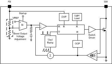 Figure 20. Boost Converter Functional Block Diagram
Both boost converters are operating at 180° phase shift to reduce current spikes from the input rail and EMI.
8.3.1.2 Protection
Three different protection schemes are implemented:
- Overvoltage protection, limits the maximum output voltage:
- Overvoltage protection limit changes dynamically based on output voltage setting. If the boost voltage is over 1.6 V higher than the adaptive control set value, the boost will stop switching.
- Keeps the output below breakdown voltage. The output voltage control limits the boost maximum voltage to 18...28 V (EPROM programmable).
- Prevents boost operation if battery voltage is much higher than desired output.
- Overcurrent protection, limits the maximum inductor current to 3.1 A (EPROM programmable).
- Duty cycle limiting.
8.3.1.3 Setting Boost Switching Frequency
The LP8555 boost converter switching frequency can be set by pre-configuring EPROM memory with the choice of boost frequency (BFREQ field). Table 1 summarizes setting of the switching frequency.
Table 1. Setting Boost Switching Frequency
| BFREQ | ƒSW [kHz] |
| 0 | 500 |
| 1 | 1000 |
8.3.1.4 Adaptive Boost Output Voltage Control
The boost converters operate in adaptive voltage control mode in typical application. The voltages at the LED terminals is monitored by the control loop. It raises the boost voltage when the measured voltage of ANY of the LED strings in a bank falls below the voltage threshold of its corresponding LOW comparator. If the headrooms of ALL of the LED strings in a bank are above the voltage threshold of their corresponding MID comparator, then the boost voltage is lowered. Both banks have independent boost voltage control to save power in case of Vf mismatch between LED strings.
The initial boost voltage is configured with the VINIT field. The VMAX field sets the maximum boost voltage. When an LED terminal is open, the monitored voltage will never have enough headroom and the adaptive mode control loop will keep raising the boost voltage. The VMAX field allows the boost voltage to be limited to stay under the voltage rating of the external components.
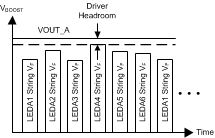 Figure 21. Boost Adaptive Control Principle for Bank A Boost Converter With Phase Shifted Outputs
8.3.1.5 EMI Reduction
The LP8555 features three EMI reduction schemes.
First scheme, Programmable Slew Rate Control, uses a combination of four drivers for boost switch. Enabling all four drivers allows boost switch on/off transition times to be the shortest. On the other hand, enabling just one driver allows boost switch on/off transition times to be the longest. The longer the transition times, the lower the switching noise on the SW node. It should also be noted that the shortest transition times bring the best efficiency as the switching losses are the lowest. Same controls effect both boost converters.
The second EMI reduction scheme is the Spread Spectrum Scheme which deliberately spreads the frequency content of the boost switching waveform, which inherently has a narrow bandwidth, makes the switching waveform's noise spectrum bandwidth wider and ultimately reduces its EMI spectral density.
The third feature for reducing EMI is Phase Shifted Clocking mode, where boost converters’ clocks are operating 180° phase shifted. This prevents boost switches switching on at the same time when operating in PWM mode. This reduces input rail load transient spikes caused by boost inductor current and gate driver currents.
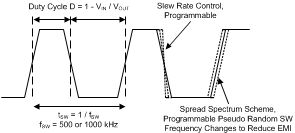 Figure 22. Boost Converter EMI Reduction Schemes
8.3.2 Brightness Control
The brightness can be controlled using an external PWM signal or the Brightness registers accessible via an I2C interface, or both. Which of these two input sources are selected is set by the BRTMODE EPROM bits. How the brightness is controlled in each of the four possible modes is described in the following sections.
8.3.2.1 PWM Input Duty Measurement
When using PWM input for brightness control the input PWM duty cycle is measured as described in following diagram and the brightness is controlled based on the result. When changing the brightness it must be noted that the measurement cycle is from rising edge to next rising edge and brightness change must be done accordingly (time from rising to rising edge is constant (=cycle time) and falling edge defines the brightness).
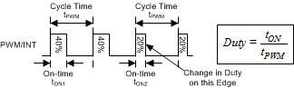 Figure 23. PWM Input Duty Cycle Measurement
8.3.2.2 BRTMODE = 00
With BRTMODE = 00, the LED output current is controlled by the PWM input duty cycle. The PWM detector block measures the duty cycle at the PWM/INT terminal and uses it to generate a PWM-based brightness code. Before the output is generated, the code goes through the curve Shaper block. Then the code goes into the Hybrid PWM and Current Dimming block which determines the range of the PWM and Current control. The outcome of the Hybrid PWM and Current Dimming block is Current and/or up to 6 PWM output signals.
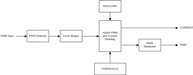 Figure 24. BRTMODE = 00 Brightness Control
8.3.2.3 BRTMODE = 01
With BRTMODE = 01, the LED output current is controlled by the BRTHI/BRTLO registers. Before the output is generated the BRTHI/BRTLO registers-based brightness code goes through the Curve Shaper block. Then the code goes into the Hybrid PWM and Current Dimming block which determines the range of the PWM and Current control. The outcome of the Hybrid PWM and Current Dimming block is Current and/or up to 6 PWM output signals.
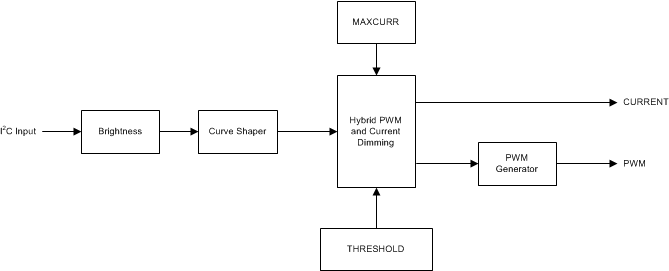 Figure 25. BRTMODE = 01 Brightness Control
8.3.2.4 BRTMODE = 10
With BRTMODE = 10, the LED output current is controlled by PWM input duty cycle and the BRTHI/BRTLO registers. The PWM detector block measures the duty cycle at the PWM/INT terminal and uses it to generate PWM-based brightness code. Before the code is multiplied with the BRTHI/BRTLO registers-based brightness code, it goes through the Curve Shaper block. After the multiplication, the resulting code goes into the Hybrid PWM and Current Dimming block which determines the range of the PWM and Current control. The outcome of the Hybrid PWM and Current Dimming block is Current and/or up to 6 PWM output signals.
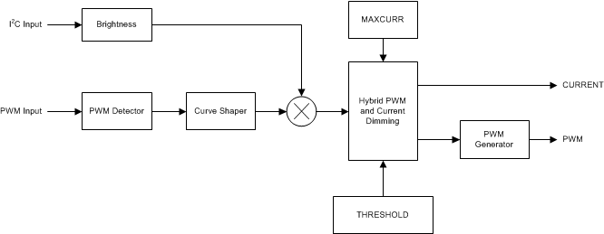 Figure 26. BRTMODE = 10 Brightness Control
8.3.2.5 BRTMODE = 11
With BRTMODE = 11, the LED output current is controlled by the PWM input duty cycle and the BRTHI/BRTLO registers. The PWM detector block measures the duty cycle at the PWM/INT terminal and uses it to generate PWM-based brightness code. In this mode, the BRTHI/BRTLO registers-based brightness code goes through the Curve Shaper block before it is multiplied with the PWM input duty cycle-based brightness code. After the multiplication, the resulting code goes into the Hybrid PWM and Current Dimming block which determines the range of the PWM and Current control. The outcome of the Hybrid PWM and Current dimming block is Current and/or up to 6 PWM output signals.
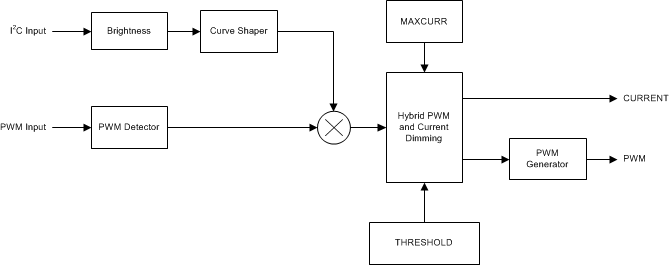 Figure 27. BRTMODE = 11 Brightness Control
8.3.2.6 Hybrid PWM and Current Dimming Control
Hybrid PWM and Current Dimming control combines PWM dimming and LED current-dimming control methods. With this dimming control, it is possible to achieve better optical efficiency from the LEDs compared to pure PWM control while still achieving smooth and accurate control and low brightness levels. The switch point from current-to-PWM control is set with THRESHOLD EPROM field, available settings are Pure PWM dimming (THRESHOLD = 111b), 25% switch point (THRESHOLD = 101b) and Pure Current Dimming (THRESHOLD = 000b). 25% setting allows good compromise between good matching of the LEDs brightness/white point at low brightness and good optical efficiency.
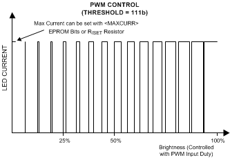 Figure 28.
 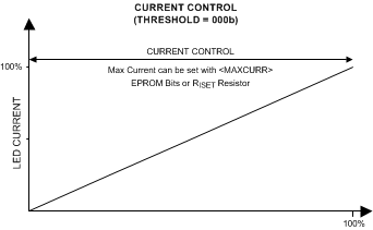 Figure 30.
 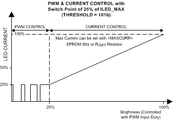 Figure 29.
 8.3.2.7 Setting PWM Dimming Frequency
The LP8555 LED PWM dimming frequency can be set either by an external resistor (PFSET = 1 selection), RFSET, or by pre-configuring EPROM memory with the choice of PWM dimming frequency (PFREQ field). Table 2 summarizes setting of the PWM dimming frequency. Setting the PWM dimming frequency using an external resistor is separately shown in Table 3.
Table 2. Setting PWM Dimming Frequency
| PFSET | RFSET | PFREQ | ƒPWM [kHz] |
|---|---|---|---|
| 1 | See Table 3 | Don't Care | See Table 3 |
| 0 | Don't Care | 000 | 4.9 |
| 0 | Don't Care | 001 | 9.8 |
| 0 | Don't Care | 011 | 19.5 |
| 0 | Don't Care | 111 | 39.1 |
Table 3. Setting PWM Dimming Frequency With an External Resistor
| PFSET | RFSET [Ω] (Tolerance) | ƒPWM [kHz] |
|---|---|---|
| 1 | 63.4k (±1%) | 4.9 |
| 1 | 52.3k, 53.6k (±1%) | 9.8 |
| 1 | 39.2k (±1%) | 19.5 |
| 1 | 23.2k (±1%) | 39.1 |
| 1 | Grounded or floating | 19.5 |
8.3.2.8 Setting Full-Scale LED Current
The LP8555 full-scale LED current can be set either by an external resistor RISET (ISET = 1 selection), or by pre-configuring EPROM memory with the choice of full-scale LED current (MAXCURR field, ISET = 0). This register can be also written with I2C before turning on backlight. Table 4 summarizes setting of the full-scale LED current.
Table 4. Setting Full-Scale LED Current
| ISET | RISET [Ω] (Tolerance) | MAXCURR | ILED [mA] |
|---|---|---|---|
| 1 | Floating | Don't Care | 23 |
| 1 | 63.4k (±1%) | Don't Care | 5 |
| 1 | 52.3k, 53.6k (±1%) | Don't Care | 10 |
| 1 | 44.2k, 45.3k (±1%) | Don't Care | 15 |
| 1 | 39.2k (±1%) | Don't Care | 20 |
| 1 | 34.0k (±1%) | Don't Care | 23 |
| 1 | 30.1k (±1%) | Don't Care | 25 |
| 1 | 26.1k (±1%) | Don't Care | 30 |
| 1 | 23.2k (±1%) | Don't Care | 50 |
| 1 | 0 (grounded) | Don't Care | 23 |
| 0 | Don't Care | 000 | 5 |
| 0 | Don't Care | 001 | 10 |
| 0 | Don't Care | 010 | 15 |
| 0 | Don't Care | 011 | 20 |
| 0 | Don't Care | 100 | 23 |
| 0 | Don't Care | 101 | 25 |
| 0 | Don't Care | 110 | 30 |
| 0 | Don't Care | 111 | 50 |
8.3.2.9 Phase-Shift PWM Scheme
The Phase-Shift PWM Scheme (PSPWM) allows delaying of the time when each LED current sink is active. When the LED current sinks are not activated simultaneously, the peak load current from the boost output is greatly decreased during PWM dimming. This reduces the ripple seen on the boost output and allows smaller output capacitors to be used. Reduced ripple also reduces the output ceramic capacitor audible ringing. The PSPWM scheme also increases the load frequency seen on the boost output by up to six times and therefore transfers the possible audible noise to the frequencies outside of the audible range.
The phase difference between each active driver is automatically determined and is 360º / number of active drivers in a bank.
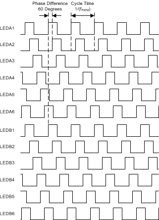 Figure 31. Phase Shifting Example With All 12 Channels Active. (Note: Bank A And Bank B are in the Same Phase.)
8.3.3 LED Brightness Slopes, Normal and Advanced
The transition time between two brightness values can be programmed with the STEP EPROM field from 0 to 200 ms. The same slope time is used for sloping up and down. With advanced slope the brightness changes can be made more pleasing to the human eye. It is implemented with a digital smoothing filter. The filter strength is set with SMOOTH EPROM field.
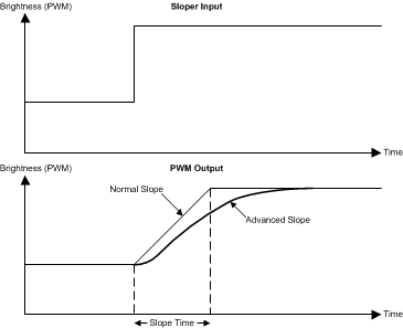 Figure 32. Sloping Principle
8.3.4 Start-up and Shutdown Sequences
Depending on brightness control mode the LP8555 can be started up or shut down differently. Below are explained typical start-up/shutdown sequences with corresponding timings for operation states. Diagrams have more details and illustrated waveforms for typical usage cases.
8.3.4.1 Start-up With PWM Input Brightness Control Mode (BRTMODE = 00b)
When VDD and EN/VDDIO are above min operational value the LP8555 enters start-up mode. During start-up mode the LDO is started, and EPROM values are read. I2C is available after the start-up sequence has ended.
In standby mode the device waits for the ON bit to go high to start the boost start-up sequence. In standby mode PWM input duty cycle measurement is active.
Once the ON bit is set to 1 (it can be also programmed to 1 by default in EPROM, and no I2C write is then needed for entering active mode), boost is started, and device enters active mode with brightness set by PWM input duty cycle. If no brightness is set, the backlight stays off until two PWM pulses are received in the PWM input, or if PWM input is set high for more than 1/75 Hz time. Boost starts initially to the level programmed in EPROM, and after backlight is turned on the adaptive control adjusts the voltage to get to the minimal headroom voltage.
8.3.4.2 Shutdown With PWM Input Brightness Control Mode (BRTMODE = 00b)
The backlight can be turned off by setting PWM input low or by writing the ON bit low. After a 1/75Hz timeout period in the PWM input, the backlight slopes down (if slope is enabled), and boost is returned to the initial voltage level programmed to the EPROM. If the backlight is shut down with the ON bit, it shuts down immediately even if slopes are enabled and boost turns off as well. To enter standby mode where boost is disabled and the power consumption is minimal, the ON bit must be written to 0. If PWMSB bit has been programmed to 1, then the LP8555 enters standby mode when PWM input has been low for more than 50 ms even if the ON bit is high.
The device shuts down completely by setting EN/VDDIO and/or VDD to low state.
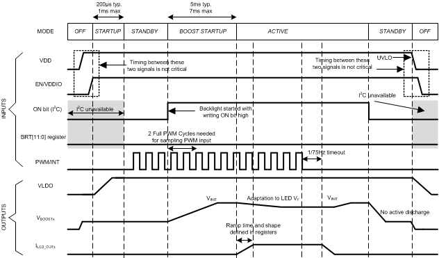 Figure 33. Start-up and Shutdown with PWM Input Control, ON Bit = 0 (BRTMODE = 00b)
 Figure 34. Start-up and Shutdown with PWM Input Control, ON Bit = 1 (BRTMODE = 00b)
8.3.4.3 Start-up With I2C Brightness Control Mode (BRTMODE = 01b)
When VDD and EN/VDDIO are above min operational value, the LP8555 enters start-up mode. During start-up mode the LDO is started, and EPROM values are read. I2C is available after the start-up sequence has ended.
In standby mode the device waits for the ON bit to go high to start the boost start-up sequence. In standby mode I2C is active, and brightness / other registers can be written.
Once the ON bit is set to 1 (it can be also programmed to 1 by default in EPROM and no I2C write is then needed for entering active mode), boost is started, and device enters active mode with brightness set by I2C brightness registers. If no brightness is set, the backlight stays off until brightness value is written to the I2C register(s). Boost starts initially to the level programmed in EPROM and, after backlight is turned on, the adaptive control adjusts the voltage to get to the minimal headroom voltage.
8.3.4.4 Shutdown With I2C Brightness Control Mode (BRTMODE = 01b)
The backlight can be turned off by setting the ON bit low, or by writing brightness to 0. The backlight shuts down immediately if the ON bit is written low even if slope is enabled. If the backlight is turned off by writing brightness to 0, brightness control does slope (if enabled), and the boost is returned to the initial voltage level programmed to EPROM. To enter standby mode where boost is disabled and the power consumption is minimal, the ON bit must be written to 0.
The device shuts down completely by setting EN/VDDIO and/or VDD to low state.
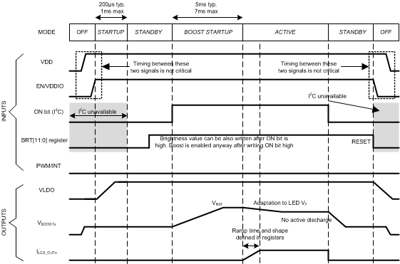 Figure 35. Start-up And Shutdown With I2C Brightness Control Mode (BRTMODE = 01b)
8.3.4.5 Start-up with I2C + PWM Input Brightness Control Mode (BRTMODE = 10 or 11b)
When VDD and EN/VDDIO are above min operational value, the LP8555 enters start-up mode. During start-up mode the LDO is started, and EPROM values are read. I2C is available after the start-up sequence has ended.
In standby mode the device waits for the ON bit to go high to start the boost start-up sequence. In standby mode I2C registers can be written and PWM input duty cycle measurement is active.
Once the ON bit is set to 1 (it can be also programmed to 1 by default in EPROM and no I2C write is then needed for entering active mode), boost is started, and device enters active mode with brightness set by PWM input duty cycle multiplied by I2C brightness register value. If no brightness is set, the backlight stays off until I2C brightness register receives value and two PWM pulses are received in the PWM input, or if PWM input is set high for more than 1/75 Hz time. Boost starts initially to the level programmed in EPROM and after backlight is turned on, the adaptive control adjusts the voltage to get to the minimal headroom voltage.
8.3.4.6 Shutdown with I2C + PWM Input Brightness Control Mode (BRTMODE = 10 or 11b)
The backlight can be turned off by setting the ON bit low, or by setting brightness to 0 either by PWM input (same 1/75 Hz timeout applies here as in PWM input control mode) or by I2C brightness register writes. The backlight shuts down immediately if the ON bit is written low even if slope is enabled. If the backlight is turned off by setting brightness to 0, brightness control does slope (if enabled, depending on which input is used – see brightness control modes for details), and the boost is returned to the initial voltage level programmed to EPROM. To enter standby mode where boost is disabled and the power consumption is minimal, the ON bit must be written to 0.
The device shuts down completely by setting EN/VDDIO and/or VDD to low state.
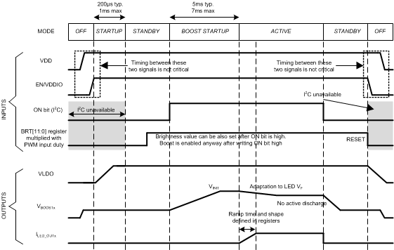 Figure 36. Start-up and Shutdown with I2C + PWM Input Brightness Control (BRTMODE = 01b)
8.3.5 LED String Count Auto Detection
The LP8555 can be pre-configured to auto-detect the number of the LED strings attached. If the CONFIG.AUTO bit is set to 1, the LP8555 will automatically remove the unused current sink and adjust phasing of the remaining current sinks. The LED OPEN fault condition will not be set in this mode.
8.3.6 Fault Detection
The LP8555 has fault detection for LED OPEN, LED SHORT, UVLO, BST_OVP, BST_OCP, BST_UV and TSD. Faults are recorded in the STATUS register. Each time the STATUS register is read, it is automatically cleared. When BRTMODE is set to 01b any fault may be enabled to cause an interrupt on the PWM/INT terminal.
8.3.6.1 LED Short Detection
Voltages at the individual current sinks are constantly monitored for the LED SHORT fault. This fault may occur when some LEDs in a string are electrically bypassed making that LED string shorter than the other LED strings. The reduced forward voltage causes the current sink attached to that string to have a higher headroom voltage than the other current sinks. When the headroom voltage is higher than the fault comparator threshold (configured with the OV field in the LEDEN register) that current sink is disabled and the PWM phasing is automatically adjusted. The fault comparator threshold may be configured for 1 V, 2 V, 3 V or 4 V.
8.3.6.2 LED Open Detection
Each current sink is also monitored for an LED OPEN condition. The condition is set when the headroom voltage on one or more current sinks is below the LOW comparator threshold and the boost voltage is at the maximum. This fault condition may be caused by one or more OPEN LED strings or by one or more current sinks shorted to GND.
The AUTO bit of the CONFIG register determines how the LP8555 responds to an LED OPEN condition. If the CONFIG.AUTO bit is set to 1, the LP8555 will automatically adjust the phasing to remove the current sink with the LED OPEN condition. In this case the condition is normal and indicates an unpopulated LED string. If the CONFIG.AUTO bit is set to 0, the LP8555 will immediately shut down the backlight whenever an LED OPEN condition is detected on any enabled LED drivers. The backlight will not turn on again (regardless of the COMMAND.ON bit) until the STATUS register is read.
8.3.6.3 Undervoltage Detection
The LP8555 continuously monitors the voltage on the VDD terminal. When the VDD voltage drops below 2.5 V the backlight will be immediately shut down, and the UVLO bit will be set in the STATUS register. The backlight will automatically start again when the voltage has increased above 2.5 V + 50 mV hysteresis. Hysteresis is implemented to avoid continuously triggering undervoltage.
8.3.6.4 Thermal Shutdown
If the internal temperature reaches 150°C, the LP8555 will immediately shut down the backlight to protect it from damage. The TSD bit will also be set in the STATUS register. The device will re-activate the backlight again when the internal temperature drops below 137°C (typ).
8.3.6.5 Boost Overcurrent Protection
The LP8555 will automatically limit boost current to 3.1 A (EPROM programmable). When the 3.1-A limit is reached the BST_OCP bit is set in the STATUS register.
8.3.6.6 Boost Overvoltage Protection
The LP8555 will automatically limit boost voltage to VBOOST_MAX+1.6 V. When the limit is reached the BST_OVP bit is set in the STATUS register. It is possible to set the limit to four threshold levels programmable via EPROM bits.
8.3.6.7 Boost Undervoltage Protection
The LP8555 can detect when the boost voltage is below VBOOST – 2.5 V for longer than 6ms. When the threshold is reached the BST_UV bit is set in the STATUS register.
8.3.7 I2C-Compatible Serial Bus Interface
8.3.7.1 Interface Bus Overview
The I2C compatible synchronous serial interface provides access to the programmable functions and registers on the device. This protocol use a two-wire interface for bi-directional communications between the IC’s connected to the bus. The two interface lines are the Serial Data Line (FSET/SDA), and the Serial Clock Line (ISET/SCL). These lines should be connected to a positive supply, via a pull-up resistor and remain HIGH even when the bus is idle.
Every device on the bus is assigned a unique address and acts as either a Master or a Slave depending on whether it generates or receives the serial clock (ISET/SCL). The LP8555 is always a slave device.
See the LP8555EVM User Guide for full register map details and programming considerations.
8.3.7.2 Data Transactions
One data bit is transferred during each clock pulse. Data is sampled during the high state of the serial clock (SCL). Consequently, throughout the clock’s high period, the data should remain stable. Any changes on the SDA line during the high state of the SCL and in the middle of a transaction, aborts the current transaction. New data should be sent during the low SCL state. This protocol permits a single data line to transfer both command/control information and data using the synchronous serial clock.
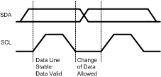 Figure 37. Bit Transfer
Each data transaction is composed of a Start Condition, a number of byte transfers (set by the software) and a Stop Condition to terminate the transaction. Every byte written to the SDA bus must be 8 bits long and is transferred with the most significant bit first. After each byte, an Acknowledge signal must follow. The following sections provide further details of this process.
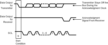 Figure 38. Start And Stop
The Master device on the bus always generates the Start and Stop Conditions (control codes). After a Start Condition is generated, the bus is considered busy and it retains this status until a certain time after a Stop Condition is generated. A high-to-low transition of the data line (SDA) while the clock (SCL) is high indicates a Start Condition. A low-to-high transition of the SDA line while the SCL is high indicates a Stop Condition.
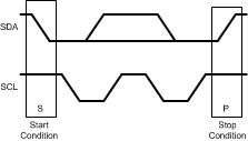 Figure 39. Start And Stop Conditions
In addition to the first Start Condition, a repeated Start Condition can be generated in the middle of a transaction. This allows another device to be accessed, or a register read cycle.
8.3.7.3 Acknowledge Cycle
The Acknowledge Cycle consists of two signals: the acknowledge clock pulse the master sends with each byte transferred, and the acknowledge signal sent by the receiving device.
The master generates the acknowledge clock pulse on the ninth clock pulse of the byte transfer. The transmitter releases the SDA line (permits it to go high) to allow the receiver to send the acknowledge signal. The receiver must pull down the SDA line during the acknowledge clock pulse and ensure that SDA remains low during the high period of the clock pulse, thus signaling the correct reception of the last data byte and its readiness to receive the next byte.
8.3.7.4 “Acknowledge After Every Byte” Rule
The master generates an acknowledge clock pulse after each byte transfer. The receiver sends an acknowledge signal after every byte received.
There is one exception to the “acknowledge after every byte” rule. When the master is the receiver, it must indicate to the transmitter an end of data by not-acknowledging (“negative acknowledge”) the last byte clocked out of the slave. This “negative acknowledge” still includes the acknowledge clock pulse (generated by the master), but the SDA line is not pulled down.
8.3.7.5 Addressing Transfer Formats
Each device on the bus has a unique slave address. The LP8555 operates as a slave device with 7-bit address combined with data direction bit. Slave address is 2Ch as 7-bit or 58h for write, and 59h for read in an 8-bit format.
Before any data is transmitted, the master transmits the address of the slave being addressed. The slave device should send an acknowledge signal on the SDA line, once it recognizes its address. The slave address is the first seven bits after a Start Condition. The direction of the data transfer (R/W) depends on the bit sent after the slave address — the eighth bit.
When the slave address is sent, each device in the system compares this slave address with its own. If there is a match, the device considers itself addressed and sends an acknowledge signal. Depending upon the state of the R/W bit (1:read, 0:write), the device acts as a transmitter or a receiver.
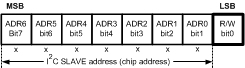 Figure 40. I2C Slave Address
8.3.7.6 Control Register Write Cycle
- Master device generates start condition.
- Master device sends slave address (7 bits) and the data direction bit (r/w = 0).
- Slave device sends acknowledge signal if the slave address is correct.
- Master sends control register address (8 bits).
- Slave sends acknowledge signal.
- Master sends data byte to be written to the addressed register.
- Slave sends acknowledge signal.
- If master will send further data bytes, the control register address will be incremented by one after acknowledge signal.
- Write cycle ends when the master creates stop condition.
8.3.7.7 Control Register Read Cycle
- Master device generates a start condition.
- Master device sends slave address (7 bits) and the data direction bit (r/w = 0).
- Slave device sends acknowledge signal if the slave address is correct.
- Master sends control register address (8 bits).
- Slave sends acknowledge signal.
- Master device generates repeated start condition.
- Master sends the slave address (7 bits) and the data direction bit (r/w = 1).
- Slave sends acknowledge signal if the slave address is correct.
- Slave sends data byte from addressed register.
- If the master device sends acknowledge signal, the control register address will be incremented by one. Slave device sends data byte from addressed register.
- Read cycle ends when the master does not generate acknowledge signal after data byte and generates stop condition.
| ADDRESS MODE | |
|---|---|
| Data Read | <Start Condition> <Slave Address><r/w = '0'>[Ack] <Register Addr.>[Ack] <Repeated Start Condition> <Slave Address><r/w = '1'>[Ack] [Register Data]<Ack or Nack>...additional reads from subsequent register address possible <Stop Condition> |
| Data Write | <Start Condition> <Slave Address><r/w = '0'>[Ack] <Register Addr.>[Ack] <Register Data>[Ack]...additional writes to subsequent register address possible <Stop Condition> |
<> Data from master; [ ] Data from slave.
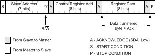 Figure 41. Register Write Format
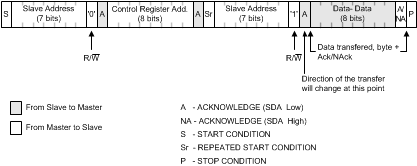 Figure 42. Register Read Format
8.4 Device Functional Modes
8.4.1 Operation Without I2C Control
The device can operate without I2C control in applications where I2C bus is not available. Special EPROM configuration is needed for this setup. In this mode the EN/VDDIO terminal enables the device, and PWM input duty cycle adjusts the brightness. Slopes, PSPWM modes, different boost modes etc. are predefined in the EPROM which device loads at start-up. FSET/SDA and ISET/SCL terminals can be used to set the PWM frequency and LED current based on specific needs (see corresponding sections for setting the frequency and current), without needing separate EPROM configuration for each application. The backlight start-up happens when EN/VDDIO terminal is high and PWM input receives measurable duty cycle. If the PWMSB bit is set 1 in EPROM, the device enters standby mode automatically when PWM/INT is set low. If PWMSB is 0, the device is shut down setting EN/VDDIO low. See start-up and shutdown diagrams for more details.
8.4.2 Operation With I2C Control
With I2C control, user may set the device configuration more freely and have additional I2C brightness control. The backlight brightness can be controlled with either PWM input, with I2C, or a combination of both. Configuration for slopes, PSPWM, or different boost modes can be used from EPROM defaults, or user can set own configuration before backlight is turned on. Configuration setting is done when EN/VDDIO is high (I2C is active) and the ON bit is low. RFSET and RISET resistors cannot be used in I2C control mode, because they are multiplexed as the I2C bus terminals (SDA/SCL). The backlight is started by setting the ON bit high, and shutdown is done by setting ON bit low. See start-up and shutdown diagrams for more details. Details of the I2C registers and programming considerations are seen in the LP8555EVM User Guide.
8.4.3 Shutdown Mode
The device is in shutdown mode when the EN/VDDIO terminal is low. the EN/VDDIO terminal enables an LDO, which is used for powering internal logic and analog blocks. Current consumption in this mode from VDD terminal is <1 µA.
8.4.4 Standby Mode
In standby mode the EN/VDDIO terminal is set high (with VDD power present), and logic is powered from an LDO. The device goes through the start-up sequence where NVM (EPROM) is loaded to the registers. I2C is available in standby mode, and register settings can be changed. Current consumption is < 30 µA in this mode from VDD terminal.
8.4.5 Active Mode
In active mode the backlight is enabled either with setting the ON register bit high (I2C control mode) or by activating PWM input. The EN/VDDIO terminal must be high, and VDD must be present. Brightness is controlled with I2C writes to brightness registers or by changing PWM input duty cycle (operation without I2C control). Configuration registers are not accessible in Active mode to prevent damage to the device by accidental writes. Current consumption from VDD terminal in this mode is typically 4.2 mA when LEDs are not drawing any current.
8.5 Register Maps
| Register | Addr | D7 | D6 | D5 | D4 | D3 | D2 | D1 | D0 |
| COMMAND | 00h | RESET | SREN | SSEN | ON | ||||
| STATUS | 01h | LED_OPEN | LED_OV | BST_UV | BST_OVP | BST_OCP | TSD | UVLO | |
| MASK | 02h | LED_OPEN | LED_OV | BST_UV | BST_OVP | BST_OCP | TSD | UVLO | |
| BRTLO | 03h | BRT[3:0] | |||||||
| BRTHI | 04h | BRT[11:4] | |||||||
| CONFIG | 10h | PWMSB | PWMFILT | EN_BPHASE180 | RELOAD | AUTO | BRTMODE | ||
| CURRENT | 11h | ISET | MAXCURR | ||||||
| PGEN | 12h | PFSET | THRESHOLD | PFREQ | |||||
| BOOST | 13h | BIND | BFREQ | ||||||
| LEDEN_0 | 14h | OV | ENABLE_0 | ||||||
| STEP | 15h | SMOOTH | PWM_IN_HYST | STEP | |||||
| VOLTAGE_0 | 16h | VMAX_0 | ADAPT_0 | VINIT_0 | |||||
| LEDEN_1 | 19h | ENABLE_1 | |||||||
| VOLTAGE_1 | 1Ah | VMAX_1 | ADAPT_1 | VINIT_1 | |||||
| OPTION | 1Ch | OPTION | |||||||
| EXTRA | 1Dh | EXTRA | |||||||
| ID | 1Eh | ID_CUST | ID_CFG | ||||||
| REVISION | 1Fh | MAJOR | MINOR | ||||||
| CONF0 | 76h | BOOST_IS_ DIV2 |
ALTID | SRON | CURR_LIMIT | ||||
| CONF1 | 77h | FMOD_DIV | |||||||
| VHR0 | 78h | VHR_SLOPE | VHR_VERT | ||||||
| VHR1 | 79h | VHR_HYST | VHR_HORZ | ||||||
| JUMP | 7Ah | JEN | JTHR | JVOLT | |||||
Some register fields are loaded from an internal EPROM (shaded above). This EPROM is programmed by TI during final test. This allows default values to be assigned. This feature is intended for applications where the I2C interface is not used. With the exception of the ID fields, all EPROM based fields can be written via I2C writes like a normal register field. There are limitations on certain configuration bits, their operation and can they be changed "on-the-fly". It is noted in the description of corresponding bit.
8.5.1 COMMAND
Address: 0x00
| D7 | D6 | D5 | D4 | D3 | D2 | D1 | D0 |
| RESET | — | SREN | SSEN | ON | |||
| Bits | Field | Type | Description |
|---|---|---|---|
| 7 | RESET | R/W | Write 1 to reset the device. This bit is self-cleaning and will always be 0 when read. |
| 6:3 | reserved | R/O | |
| 2 | SREN | R/W | 0 = Slew rate limited disabled 1 = Enable slower boost gate drive slew rate. Reduces EMI energy in high frequencies and reduces boost efficiency. |
| 1 | SSEN | R/W | 0 = Spread Spectrum Scheme disabled 1 = Enable spread-spectrum boost clocking. Spreads EMI spectrum spikes. |
| 0 | ON | R/W | Turn on the backlight. 0 = backlight off 1 = backlight on |
The COMMAND.ON bit must be programmed to 1 in the EPROM for applications without I2C access to the device. The COMMAND.SSEN bit may be updated at any time. It is not necessary for the backlight to be off when changing COMMAND.SSEN and/or COMMAND.SREN.
8.5.2 STATUS/MASK
Address: 0x01/0x02
| D7 | D6 | D5 | D4 | D3 | D2 | D1 | D0 |
| DRV_FAULT | DRV_OV | — | BST_UV | BST_OVP | BST_OCP | TSD | UVLO |
| Bits | Field | Type | Description |
|---|---|---|---|
| 7 | LED_OPEN | R/O | An open/short condition was detected on one or more LED strings. Once set this bit will stay set until the STATUS register is read. An LED open/short condition will turn off the backlight when CONFIG.AUTO is 0. |
| 6 | LED_OV | R/O | An overvoltage condition was detected on one or more LED strings. Once set this bit will stay set until the STATUS register is read. |
| 5 | reserved | R/O | |
| 4 | BST_UV | R/O | The boost reported an undervoltage condition. Once set this bit will stay set until the STATUS register is read. |
| 3 | BST_OVP | R/O | The boost reported an overvoltage protection condition when the maximum allowed voltage is requested. Once set this bit will stay set until the STATUS register is read. |
| 2 | BST_OCP | R/O | The boost reported an undervoltage condition longer than 50 ms in time when the backlight on. |
| 1 | TSD | R/O | A thermal shutdown condition was detected. Once set this bit will stay set until the STATUS register is read. A thermal shutdown condition will turn off the backlight. |
| 0 | UVLO | R/O | An undervoltage lockout condition was detected. Once set this bit will stay set until the STATUS register is read. An undervoltage lockout condition will turn off the backlight. |
Each fault bit of the STATUS register has a corresponding bit in the MASK register, which enables interrupts for the fault. For example, an interrupt will occur if the MASK.BST_UV and STATUS.BST_UV bits are both set. If a fault bit is cleared in the MASK register then that fault will not trigger an interrupt.
8.5.3 BRTLO
Address: 0x03
| D7 | D6 | D5 | D4 | D3 | D2 | D1 | D0 |
| BRT[3:0] | RESERVED |
| Bits | Field | Type | Description |
|---|---|---|---|
| 7:4 | BRT[3:0] | R/W | Least significant bits of the brightness level. |
| 3:0 | reserved | R/O |
8.5.4 BTHI
Address: 0x04
| D7 | D6 | D5 | D4 | D3 | D2 | D1 | D0 |
| BRT[11:4] |
| Bits | Field | Type | Description |
|---|---|---|---|
| 7:0 | BRT[11:4] | R/W | Most significant bits of the brightness level. |
The brightness level can be updated with 8-bit precision or 12-bit precision. To make brightness level updates effective the internal brightness level is only updated when the BRTHI register is written. If the BRTHI register is written without a previous write to the BRTLO register, then the lower 4 bits of the internal 12-bit brightness will be synthesized from the BRTHI register value.
| BRTLO | BRTHI | Brightness | Comments |
| write 0x95 | write 0xFC | 0xFC9 | BRTLO[3:0] is ignored |
| write 0x10 | write 0xDC | 0xDC1 | set to an exact 12-bit value |
| no write | write 0x8C | 0x8C8 | synthesize low order bits |
| no write | write 0x0C | 0x0C0 | synthesize low order bits |
| no write | write 0x00 | 0x000 | 0% brightness |
| no write | write 0xFF | 0xFFF | 100% brightness |
8.5.5 CONFIG
Address: 0x10
| D7 | D6 | D5 | D4 | D3 | D2 | D1 | D0 |
| PWMSB | PWMFILT | EN_BPHASE180 | RESERVED | RELOAD | AUTO | BRTMODE | |
| Bits | Field | Type | Description |
|---|---|---|---|
| 7 | PWMSB | R/W | Enables PWM standby mode 0 = CONTROL.ON alone turns the backlight on/off 1 = turn off the backlight after 50 ms of PWM low |
| 6 | PWMFILT | R/W | 0 = PWM input filter disabled 1 = Enable 50 ns glitch filter on PWM input. |
| 5 | EN_BPHASE180 | R/W | 0 = Boosts operate in same phase 1 = Enable 180° phase shift between the 2 boost switchers. |
| 4 | reserved | R/O | |
| 3 | RELOAD | R/W | Automatically re-read the EPROM at each turn-on. 0 = only read the EPROM upon power-up 1 = re-read the EPROM when the backlight turns on |
| 2 | AUTO | R/W | Automatic LED string configuration 0 = enable LED strings using just LEDEN.ENABLE 1 = disable all open LED strings |
| 1:0 | BRTMODE | R/W | Brightness mode 00 = PWM 01 = BRTHI/BRTLO registers 10 = PWM × unshaped BRTHI/BRTLO registers 11 = BRTHI/BRTLO registers × unshaped PWM |
When the AUTO bit is set the LED configuration is done dynamically. When an OPEN/SHORT condition is detected on an LED string it will be removed, and PWM output phasing will be adjusted. Conversely, an LED string will be added back for operation if the LED string is not open.
The BRTMODE field selects how LED brightness is controlled. When BRTMODE is set to 00b the PWM/INT terminal duty cycle controls the LED brightness. When BRTMODE is set to 01b the BRTLO and BRTHI registers will control the LED brightness. When the backlight is turned on the brightness level is reset to 0% and will automatically transition to the brightness value programmed in the BRTLO and BRTHI registers.
When the BRTMODE field is set to 00b, and the PWMSB bit is set to 1, the backlight will be turned off whenever the PWM/INT terminal is held low for 50 ms. This will also put the device into its lowest power state. When the PWM/INT terminal becomes active the backlight will automatically turn back on.
A 50 ns glitch filter will be applied to the PWM input signal when the PWMFILT bit is set to 1. When BRTMODE is set to 10b or 11b the LED brightness is controlled by both the PWM/INT terminal duty cycle and the BRTLO and BRTHI registers.
When BRTMODE is set to 10b the PWM/INT terminal duty cycle is routed through the smoothing function (controlled via the STEP register). The smoothed duty cycle is multiplied with the value from the BRTLO/BRTHI registers. Updates to the BRTLO/BRTHI registers have an immediate effect on the LED brightness, while PWM/INT terminal duty cycle changes may be smoothed.
When BRTMODE is set to 11b the BRTLO/BRTHI register value is routed through the smoothing function. The smoothed brightness level is multiplied with the PWM/INT terminal duty cycle. In this configuration PWM/INT terminal duty cycle changes have an immediate effect on the LED brightness, while BRTLO/BRTHI register changes may be smoothed.
8.5.6 CURRENT
Address: 0x11
| D7 | D6 | D5 | D4 | D3 | D2 | D1 | D0 |
| ISET | — | MAXCURR | |||||
| Bits | Field | Type | Description |
|---|---|---|---|
| 7 | ISET | R/W | 0 = LED maximum current set with MAXCURR bits 1 = Set MAXCURR via the ISET/SCL terminal. This terminal should only set to 1 as an EPROM default, writing to this bit "on-the-fly" does not have effect. Resistor values and their corresponding LED current setting is seen in Full-Scale LED Current section. |
| 6:3 | reserved | R/O | |
| 2:0 | MAXCURR | R/W | Full-scale current, 100% brightness (typical). 000 = 5 mA 001 = 10 mA 010 = 15 mA 011 = 20 mA 100 = 23 mA 101 = 25 mA 110 = 30 mA 111 = 50 mA |
The full-scale current can be configured into two different ways: EPROM or ISET/SCL terminal. The ISET/SCL terminal resistor is automatically measured during start-up. The CURRENT.ISET bit is used to select between the maximum current value measured from the ISET/SCL terminal and the EPROM value. When the ISET bit is set to 1 the ISET/SCL terminal value is used; otherwise the EPROM value is used. Regardless of EPROM programming, the maximum current can always be configured from I2C by clearing the CURRENT.ISET bit and configuring the CURRENT.MAXCURR field as needed.
When the CURRENT register is read via I2C the MAXCURR field will contain the active full-scale current value. To read the EPROM value the ISET bit must be set to 0. To read the RISET resistor value the ISET bit must be set to 1 during start-up, which means it must be set in EPROM.
If the ISET/SCL terminal is grounded or floating the MAXCURR value will be set to 23 mA if ISET = 1.
8.5.7 PGEN
Address: 0x12
| D7 | D6 | D5 | D4 | D3 | D2 | D1 | D0 |
| PFSET | RESERVED | THRESHOLD | PFREQ | ||||
| Bits | Field | Type | Description |
|---|---|---|---|
| 7 | PFSET | R/W | 0 = PWM frequency is set with PFREQ register bits 1 = Set PFREQ via the FSET/SDA terminal. This bit should only be set to 1 as an EPROM default, writing to this bit "on-the-fly" does not have effect. Resistor values and their corresponding frequency settings are seen in Setting PWM Dimming Frequency section. |
| 6 | RESERVED | R/O | 0 |
| 5:3 | THRESHOLD | R/W | Adaptive dimming threshold. PWM dimming is used below the threshold and current dimming is used above the threshold. 000 = 100% current dimming 101 = PWM below 25% (10-bit PWM) 111 = 100% PWM (12-bit PWM) |
| 2:0 | PFREQ | R/W | PWM output frequency (typical) 000 = 4.9 kHz 001 = 9.8 kHz 011 = 19.5 kHz 111 = 39.1 kHz |
The output PWM frequency can be configured in two different ways: EPROM or FSET/SDA terminal. The FSET/SDA terminal is always automatically measured. The PGEN.PFSET bit is used to select between the PWM frequency value measured from the FSET/SDA terminal and the EPROM value. When the PFSET bit is set to 1 the FSET/SDA terminal value is used; otherwise the EPROM value is used. Regardless of EPROM programming, the PWM frequency can always be configured from I2C by clearing the PGEN.PFSET bit and configuring the PGEN.PFREQ field as needed.
Full 12-bit precision is achieved in all adaptive dimming thresholds and PWM output frequencies. When the PGEN register is read via I2C the PFREQ field will contain the active PWM output frequency value. To read the EPROM value the PFSET bit must be set to 0. To read the RFSET resistor value the PFSET bit must be set to 1.
If the FSET/SDA terminal is grounded or floating the PFREQ value will be set to 19.5 kHz.
8.5.8 BOOST
Address: 0x13
| D7 | D6 | D5 | D4 | D3 | D2 | D1 | D0 |
| RESERVED | RESERVED | RESERVED | BIND | BFREQ | |||
| Bits | Field | Type | Description |
|---|---|---|---|
| 7:6 | RESERVED | R/W | |
| 5:4 | RESERVED | R/W | |
| 3:2 | RESERVED | R/W | |
| 1 | BIND | R/W | BIND bit is used to set boost inductor size. 0 = 4.7 µH … 6.8 µH 1 = 10 µH … 22 µH |
| 0 | BFREQ | R/W | Boost frequency (typical). This setting must be configured in EPROM, changing it with I2C register write does not have desired effect. 0 = 500 kHz 1 = 1 MHz |
8.5.9 LEDEN
Address: 0x14
| D7 | D6 | D5 | D4 | D3 | D2 | D1 | D0 |
| OV | ENABLE[6:1] | ||||||
| Bits | Field | Type | Description |
|---|---|---|---|
| 7:6 | OV | R/W | Set LED overvoltage level (typical). 00 = 1V 01 = 2V 10 = 3V 11 = 4V |
| 5:0 | ENABLE | R/W | LED string enables for Bank A. |
The ENABLE field configures the enabled LED strings. If the CONFIG.AUTO bit is 0 these LED strings will stay active when the backlight is on. If the CONFIG.AUTO bit is set, then an LED open/short condition will cause that LED string to be removed. A given LED string will never be enabled if the corresponding bit of the ENABLE field is set to 0. The OV field configures the threshold for detecting an LED overvoltage condition; which may occur when one or more LEDs are bypassed (shorted) within an LED string.
8.5.10 STEP
Address: 0x15
| D7 | D6 | D5 | D4 | D3 | D2 | D1 | D0 |
| SMOOTH | PWM_IN_HYST | STEP | |||||
| Bits | Field | Type | Description |
|---|---|---|---|
| 7:6 | SMOOTH | R/W | Advanced Slope control. Filter strength for digital smoothing filter. 00 = no smoothing 01 = light smoothing 10 = medium smoothing 11 = heavy smoothing |
| 5:2 | PWM_IN_HYST | R/W | PWM input hysteresis 000 = None 001 = >1 LSB steps 010 = >2 LSB steps 011 = >4 LSB steps 100 = >8 LSB steps 101 = >16 LSB steps 110 = >32 LSB steps 111 = >64 LSB steps |
| 2:0 | STEP | R/W | Linear Sloping time (typical) 000 = 0 ms 001 = 8 ms 010 = 16 ms 011 = 24 ms 100 = 28 ms 101 = 32 ms (12.2 µs / 12-bit LSB) 110 = 100 ms (24.4 µs / 12-bit LSB) 111 = 200 ms (48.8 µs / 12-bit LSB) |
The STEP field controls the rate of brightness level changes. Brightness transitions have a fixed step time. The time required to complete a ramp between two levels is independent upon the difference between the starting and ending current levels. For example, when STEP is set to 110b a brightness transition between any brightness values will take 100 ms. The SMOOTH field controls the digital smoothing filter, Advanced Sloping. This filter behaves much like an RC filter. It can be used to remove the overshoot that appears to occur (for eye) on large brightness changes. The actual amount of smoothing is tailored for the STEP field setting. For example medium filter strength is higher for 100 ms ramp times than for 32 ms Linear Sloping times. This gives 32 possible brightness level ramping configurations.
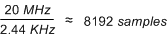
The PWM detector over-samples the input PWM signal at 20 MHz. The accuracy of the duty-cycle measurement depends upon the frequency of the PWM signal. The maximum possible accuracy is 12-bit precision. To allow 12-bit precision the LP8555 must take at least 8192 samples.
| 0 | 2.4 kHz | 4.8 kHz | 9.6 kHz | 19.5 kHz | 39 kHz | 78 kHz | 156 kHz |
| 12-bit | 11-bit | 10-bit | 9-bit | 8-bit | 7-bit | 6-bit | |
When the PWM detector detects new PWM-value, it is effective only when it differs from previous value more than selected hysteresis. Hysteresis is selected with PWM_IN_HYST in register 0x15.
8.5.11 Brightness Transitions, Typical Times
| STEP | SMOOTH | RAMP TIME (0 to 100%) (ms) |
| 000 | 00 | 0.0 |
| 000 | 01 | 0.9 |
| 000 | 10 | 1.7 |
| 000 | 11 | 3.4 |
| 001 | 00 | 8.2 |
| 001 | 01 | 14.6 |
| 001 | 10 | 22.3 |
| 001 | 11 | 38.7 |
| 010 | 00 | 16.0 |
| 010 | 01 | 28.4 |
| 010 | 10 | 43.5 |
| 010 | 11 | 75.5 |
| 011 | 00 | 24.2 |
| 011 | 01 | 42.9 |
| 011 | 10 | 65.8 |
| 011 | 11 | 114.2 |
| 100 | 00 | 27.9 |
| 100 | 01 | 49.5 |
| 100 | 10 | 75.8 |
| 100 | 11 | 131.7 |
| 101 | 00 | 32.0 |
| 101 | 01 | 56.8 |
| 101 | 10 | 87.0 |
| 101 | 11 | 151.1 |
| 110 | 00 | 102.0 |
| 110 | 01 | 181.0 |
| 110 | 10 | 277.2 |
| 110 | 11 | 481.5 |
| 111 | 00 | 204.8 |
| 111 | 01 | 363.4 |
| 111 | 10 | 556.6 |
| 111 | 11 | 966.9 |
8.5.12 VOLTAGE_0
Address: 0x16
| D7 | D6 | D5 | D4 | D3 | D2 | D1 | D0 |
| VMAX | ADAPT | VINIT | |||||
| Bits | Field | Type | Description |
|---|---|---|---|
| 7:6 | VMAX | R/W | Maximum boost voltage for Boost A (typical). 00 = 18V 01 = 22V 10 = 25V 11 = 28V |
| 5 | ADAPT | R/W | Enable adaptive headroom optimization. |
| 4:0 | VINIT | R/W | Initial boost voltage. When ADAPT is 0 the boost voltage will remain at the VINIT setting. The voltage range is from 7V to 28V; where 0x00 equals 7V and 0x3F equals 28V (typical). |
The VOLTAGE_0.VMAX bit sets the maximum allowed boost voltage for Boost A. The boost control loop will never request a higher voltage than the VMAX value. When the VOLTAGE.ADAPT bit is set to 1 the boost voltage may vary from 7V to the VMAX configured voltage.
| VINIT (DEC) | Voltage (V) | VINIT (DEC) | Voltage (V) | VINIT (DEC) | Voltage (V) |
| 0 | 7.00 | 11 | 14.45 | 22 | 21.91 |
| 1 | 7.68 | 12 | 15.13 | 23 | 22.58 |
| 2 | 8.35 | 13 | 15.8 | 24 | 23.26 |
| 3 | 9.03 | 14 | 16.48 | 25 | 23.94 |
| 4 | 9.71 | 15 | 17.16 | 26 | 24.61 |
| 5 | 10.39 | 16 | 17.84 | 27 | 25.29 |
| 6 | 11.06 | 17 | 18.52 | 28 | 25.97 |
| 7 | 11.74 | 18 | 19.2 | 29 | 26.65 |
| 8 | 12.42 | 19 | 19.87 | 30 | 27.32 |
| 9 | 13.09 | 20 | 20.55 | 31 | 28.00 |
| 10 | 13.77 | 21 | 21.23 |
Example: For system where is 7 LEDs in series with 2.9 V Vf. Target value for boost initial voltage would be: 7 x (2.9 V + 0.1 V) + 2 V = 23 V → VINIT = 24(DEC). 0.1 V represents Vf variation of single LED, and 2 V is worst case headroom. So it is desirable to set the initial voltage little higher than the actual Vf voltage to take the worst-case condition in consideration.
8.5.13 LEDEN1
Address: 0x19
| D7 | D6 | D5 | D4 | D3 | D2 | D1 | D0 |
| RESERVED | ENABLE[6:1] | ||||||
| Bits | Field | Type | Description |
|---|---|---|---|
| 7:6 | RESERVED | R/O | |
| 5:0 | ENABLE1 | R/W | LED string enables for Bank B. |
The ENABLE field configures the enabled LED strings. If the CONFIG.AUTO bit is 0 these LED strings will stay active when the backlight is on. If the CONFIG.AUTO bit is set, then an LED open/short condition will cause that LED string to be removed. A given LED string will never be enabled if the corresponding bit of the ENABLE field is set to 0. The OV field configures the threshold for detecting an LED overvoltage condition; which may occur when one or more LEDs are bypassed (shorted) within an LED string.
8.5.14 VOLTAGE1
Address: 0x1A
| D7 | D6 | D5 | D4 | D3 | D2 | D1 | D0 |
| VMAX1 | ADAPT1 | VINIT1 | |||||
| Bits | Field | Type | Description |
|---|---|---|---|
| 7:6 | VMAX | R/W | Maximum boost voltage for Boost B (typical). 00 = 18 V 01 = 22 V 10 = 25 V 11 = 28 V |
| 5 | ADAPT | R/W | Enable adaptive headroom optimization. |
| 4:0 | VINIT1 | R/W | Initial boost voltage. When ADAPT is 0 the boost voltage will remain at the VINIT setting. The voltage range is from 7 V to 28 V; where 0x00 equals 7 V and 0x3F equals 28 V (typical). |
The VOLTAGE1.VMAX bit sets the maximum allowed boost voltage for Boost B. The boost control loop will never request a higher voltage than the VMAX value. When the VOLTAGE.ADAPT bit is set to 1 the boost voltage may vary from 7 V to the VMAX configured voltage.
| VINIT (DEC) | VOLTAGE (V) | VINIT (DEC) | VOLTAGE (V) | VINIT (DEC) | VOLTAGE (V) |
| 0 | 7.00 | 11 | 14.45 | 22 | 21.91 |
| 1 | 7.68 | 12 | 15.13 | 23 | 22.58 |
| 2 | 8.35 | 13 | 15.8 | 24 | 23.26 |
| 3 | 9.03 | 14 | 16.48 | 25 | 23.94 |
| 4 | 9.71 | 15 | 17.16 | 26 | 24.61 |
| 5 | 10.39 | 16 | 17.84 | 27 | 25.29 |
| 6 | 11.06 | 17 | 18.52 | 28 | 25.97 |
| 7 | 11.74 | 18 | 19.2 | 29 | 26.65 |
| 8 | 12.42 | 19 | 19.87 | 30 | 27.32 |
| 9 | 13.09 | 20 | 20.55 | 31 | 28.00 |
| 10 | 13.77 | 21 | 21.23 |
8.5.15 OPTION
Address: 0x1C
| D7 | D6 | D5 | D4 | D3 | D2 | D1 | D0 |
| RESERVED | OPTION |
| Bits | Field | Type | Description |
|---|---|---|---|
| 7:4 | reserved | R/O | |
| 3:0 | OPTION | R/O | Metal option identifier. |
8.5.16 EXTRA
Address: 0x1D
| D7 | D6 | D5 | D4 | D3 | D2 | D1 | D0 |
| EXTRA |
| Bits | Field | Type | Description |
|---|---|---|---|
| 7:0 | EXTRA | R/W | User accessible extra identifier register |
8.5.17 ID
Address: 0x0E
| D7 | D6 | D5 | D4 | D3 | D2 | D1 | D0 |
| ID_CUST | ID_CFG |
| Bits | Field | Type | Description |
|---|---|---|---|
| 7:4 | ID_CUST | R/W | TI Customer ID code. |
| 3:0 | ID_CFG | R/W | TI Configuration ID code. |
The ID field is configured by TI when the EPROM is programmed.
8.5.18 REVISION
Address: 0x0F
| D7 | D6 | D5 | D4 | D3 | D2 | D1 | D0 |
| MAJOR | MINOR |
| Bits | Field | Type | Description |
|---|---|---|---|
| 7:4 | MAJOR | R/O | Major silicon revision. |
| 3:0 | MINOR | R/O | Minor silicon revision. |
The REVISION register provides silicon revision information in case test SW needs to distinguish between different revisions of the device or later identification is needed. REVISION register content comes from read only metal register (connected at COM level).
8.5.19 CONF0
Address: 0x76
| D7 | D6 | D5 | D4 | D3 | D2 | D1 | D0 |
| BOOST_IS_DIV2 | RESERVED | ALTID | SRON | CURR_LIMIT | |||
| Bits | Field | Type | Description |
|---|---|---|---|
| 7 | BOOST_IS_DIV2 | R/W | Divide inductor peak current by 2 0 = Normal operation 1 = Inductor currents divided by 2 |
| 6:5 | RESERVED | R/W | |
| 4 | ALTID | R/W | I2C Slave ID selector 0 = 2Ch 1 = 2Eh |
| 3:2 | SRON | R/W | Slowed boost slew rate. When COMMAND.SREN is set to 1 boost slew rate is controlled with this value. |
| 1:0 | CURR_LIMIT | R/W | Boost inductor peak current limit (typical). BOOST_IS_DIV2 sets which of the limits is used. 00 = 0.9 A / 1.55 A 01 = 1.2 A / 2.1 A 10 = 1.5 A / 2.6 A 11 = 1.8 A / 3.1 A |
8.5.20 CONF1
Address: 0x77
| D7 | D6 | D5 | D4 | D3 | D2 | D1 | D0 |
| FMOD_DIV | RESERVED | RESERVED | RESERVED |
| Bits | Field | Type | Description |
|---|---|---|---|
| 7:6 | FMOD_DIV | R/W | Spread spectrum modulation frequency divisor. 00 = 0.45% 01 = 0.27% 10 = 0.17% 11 = 0.12% |
| 5:0 | RESERVED | R/W |
The FMOD_DIV field controls modulation frequency for spread spectrum clocking. The actual modulation frequency scales with the boost frequency.
| BOOST FREQUENCY (kHz) | FMOD_DIV = 00b (kHz) | FMOD_DIV = 01b (kHz) | FMOD_DIV = 10b (kHz) | FMOD_DIV = 11b (kHz) |
|---|---|---|---|---|
| 1000 | 4.17 | 2.78 | 1.67 | 1.19 |
| 500 | 2.08 | 1.39 | 0.83 | 0.64 |
8.5.21 VHR0
Address: 0x78
| D7 | D6 | D5 | D4 | D3 | D2 | D1 | D0 |
| RESERVED | VHR_SLOPE | RESERVED | VHR_VERT | ||||
| Bits | Field | Type | Description |
|---|---|---|---|
| 7 | RESERVED | R/O | |
| 6:4 | VHR_SLOPE | R/W | Typical headroom voltage at maximum current (50 mA) 000 = 210 mV 001 = 223 mV 010 = 235 mV 011 = 248 mV 100 = 260 mV 101 = 273 mV 110 = 285 mV 111 = 300 mV |
| 3 | RESERVED | ||
| 2:0 | VHR_VERT | R/W | Typical minimum headroom voltage 000 = 50 mV 001 = 80 mV 010 = 110 mV 011 = 140 mV 100 = 170 mV 101 = 200 mV 110 = 230 mV 111 = 260 mV |
8.5.22 VHR1
Address: 0x79
| D7 | D6 | D5 | D4 | D3 | D2 | D1 | D0 |
| RESERVED | VHR_HYST | RESERVED | VHR_HORZ |
| Bits | Field | Type | Description |
|---|---|---|---|
| 7:6 | RESERVED | R/O | |
| 5:4 | VHR_HYST | R/W | Typical hysteresis for the mid comparator threshold (above the low comparator threshold). 00 = 200 mV 01 = 233 mV 10 = 466 mV 11 = 600 mV |
| 3:2 | RESERVED | R/O | |
| 1:0 | VHR_HORZ | R/W | Percentage of full driver range (horizontal component) 00 = 1% 01 = 25% 10 = 37.5% 11 = 50% |
8.5.23 JUMP
Address: 0x7A
| D7 | D6 | D5 | D4 | D3 | D2 | D1 | D0 |
| JEN | RESERVED | JTHR | JVOLT | ||||
| Bits | Field | Type | Description |
|---|---|---|---|
| 7 | JEN | R/W | Enable boost voltage jumping on large brightness percentage increases. |
| 6:4 | RESERVED | R/W | |
| 3:2 | JTHR | R/W | Jump brightness percentage threshold. 00 = 6.25% 01 = 12.5% 10 = 25% 11 = 50% |
| 1:0 | JVOLT | R/W | Typical Boost voltage jump size (10.26 mV/step) 00 = 195 steps (2 V) 01 = 390 steps (4 V) 10 = 585 steps (6 V) 11 = 780 steps (8 V) |
The jump feature operates outside of the normal adaptive headroom loop. Whenever the brightness percentage instantaneously increases above the configured threshold the boost voltage is instructed to immediately jump up. This can be used in some rare cases where extremely fast boost reaction time to brightness changes is needed. The JTHR field configures the threshold and the JVOLT field configures the voltage increase. The requested boost voltage will never exceed the value set by the VOLTAGE.VMAX field.