SNVSBC7 August   2019 LP8867C-Q1 , LP8869C-Q1

PRODUCTION DATA.  

  1. Features
    1.     Simplified Schematic
  2. Applications
  3. Description
    1.     System Efficiency
  4. Revision History
  5. Device Comparison Table
  6. Pin Configuration and Functions
    1.     Pin Functions
  7. Specifications
    1. 7.1  Absolute Maximum Ratings
    2. 7.2  ESD Ratings
    3. 7.3  Recommended Operating Conditions
    4. 7.4  Thermal Information
    5. 7.5  Electrical Characteristics
    6. 7.6  Internal LDO Electrical Characteristics
    7. 7.7  Protection Electrical Characteristics
    8. 7.8  Current Sinks Electrical Characteristics
    9. 7.9  PWM Brightness Control Electrical Characteristics
    10. 7.10 Boost and SEPIC Converter Characteristics
    11. 7.11 Logic Interface Characteristics
    12. 7.12 Typical Characteristics
  8. Detailed Description
    1. 8.1 Overview
    2. 8.2 Functional Block Diagram
    3. 8.3 Feature Description
      1. 8.3.1 Integrated DC-DC Converter
        1. 8.3.1.1 DC-DC Converter Parameter Configuration
          1. 8.3.1.1.1 Switching Frequency
          2. 8.3.1.1.2 Spread Spectrum and External SYNC
          3. 8.3.1.1.3 Recommended Component Value and Internal Parameters
          4. 8.3.1.1.4 DC-DC Converter Switching Current Limit
          5. 8.3.1.1.5 DC-DC Converter Light Load Mode
        2. 8.3.1.2 Adaptive Voltage Control
          1. 8.3.1.2.1 Using Two-Divider
          2. 8.3.1.2.2 Using T-Divider
          3. 8.3.1.2.3 Feedback Capacitor
      2. 8.3.2 Internal LDO
      3. 8.3.3 LED Current Sinks
        1. 8.3.3.1 LED Output Configuration
        2. 8.3.3.2 LED Current Setting
        3. 8.3.3.3 Brightness Control
      4. 8.3.4 Protection and Fault Detections
        1. 8.3.4.1 Supply Fault and Protection
          1. 8.3.4.1.1 VIN Undervoltage Fault (VIN_UVLO)
          2. 8.3.4.1.2 VIN Overvoltage Fault (VIN_OVP)
        2. 8.3.4.2 Boost Fault and Protection
          1. 8.3.4.2.1 Boost Overvoltage Fault (BST_OVP)
          2. 8.3.4.2.2 SW Overvoltage Fault (SW_OVP)
        3. 8.3.4.3 LED Fault and Protection
          1. 8.3.4.3.1 LED Open Fault (LED_OPEN)
          2. 8.3.4.3.2 LED Short Fault (LED_SHORT)
        4. 8.3.4.4 Thermal Fault and Protection (TSD)
        5. 8.3.4.5 Overview of the Fault and Protection Schemes
    4. 8.4 Device Functional Modes
      1. 8.4.1 STANDBY State
      2. 8.4.2 SOFT START State
      3. 8.4.3 BOOST START State
      4. 8.4.4 NORMAL State
      5. 8.4.5 FAULT RECOVERY State
      6. 8.4.6 State Diagram and Timing Diagram for Start-up and Shutdown
  9. Application and Implementation
    1. 9.1 Application Information
    2. 9.2 Typical Applications
      1. 9.2.1 Typical Application for 4 LED Strings
        1. 9.2.1.1 Design Requirements
        2. 9.2.1.2 Detailed Design Procedure
          1. 9.2.1.2.1 Inductor Selection
          2. 9.2.1.2.2 Output Capacitor Selection
          3. 9.2.1.2.3 Input Capacitor Selection
          4. 9.2.1.2.4 LDO Output Capacitor
          5. 9.2.1.2.5 Diode
        3. 9.2.1.3 Application Curves
      2. 9.2.2 SEPIC Mode Application
        1. 9.2.2.1 Design Requirements
        2. 9.2.2.2 Detailed Design Procedure
          1. 9.2.2.2.1 Inductor
          2. 9.2.2.2.2 Diode
          3. 9.2.2.2.3 Capacitor C1
        3. 9.2.2.3 Application Curves
  10. 10Power Supply Recommendations
  11. 11Layout
    1. 11.1 Layout Guidelines
    2. 11.2 Layout Example
  12. 12Device and Documentation Support
    1. 12.1 Device Support
      1. 12.1.1 Development Support
    2. 12.2 Documentation Support
      1. 12.2.1 Related Documentation
    3. 12.3 Receiving Notification of Documentation Updates
    4. 12.4 Community Resources
    5. 12.5 Trademarks
    6. 12.6 Electrostatic Discharge Caution
    7. 12.7 Glossary
  13. 13Mechanical, Packaging, and Orderable Information

Package Options

Mechanical Data (Package|Pins)
Thermal pad, mechanical data (Package|Pins)
Orderable Information

LED Short Fault (LED_SHORT)

Shorted LED fault is detected if one or more LED outputs are above the VHIGH_COMP threshold (typical 6 V) and at least one LED output is inside the normal operation window (between VLOW_COMP and VMID_COMP, typical 0.9 V and 1.9 V). The shorted string is disconnected from the boost adaptive control loop and its output is disabled.

LED Open fault detection and LED Short fault detection are available only in NORMAL state.
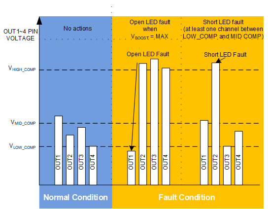
LP8867C-Q1 LP8869C-Q1 cht-02-adaptive-fault.gifFigure 15. Protection and DC-DC Voltage Adaptation Algorithms

If LED fault is detected, the device continues normal operation and only the faulty string is disabled. The fault is indicated via the FAULT pin which can be released by toggling VDDIO/EN pin low for a short period of 2 µs to 20 µs. LEDs are turned off for this period but the device stays in NORMAL state. If VDDIO/EN is low longer, the device goes to STANDBY and restarts when EN goes high again.

This means if the system doesn't want to simply disable the device because of LED faults. It could clear the LED faults by toggling VDDIO/EN pin low for a short period of 2 µs to 20 µs.