SNOSCX9A March 2015 – November 2015 LPV542
PRODUCTION DATA.
- 1 Features
- 2 Applications
- 3 Description
- 4 Revision History
- 5 Pin Configuration and Functions
- 6 Specifications
- 7 Detailed Description
- 8 Application and Implementation
- 9 Power Supply Recommendations
- 10Layout
- 11Device and Documentation Support
- 12Mechanical, Packaging, and Orderable Information
Package Options
Mechanical Data (Package|Pins)
Thermal pad, mechanical data (Package|Pins)
Orderable Information
5 Pin Configuration and Functions
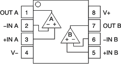
8-Pin VSSOP
DGK Package
Top View

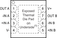
8-Pad X1SON
DNX Package
Top View

1. Connect thermal die pad to V-.
Pin Functions
| PIN | I/O | DESCRIPTION | |||
|---|---|---|---|---|---|
| NAME | DGK | DNX | |||
| OUT A | 1 | 1 | O | Channel A Output | |
| -IN A | 2 | 2 | I | Channel A Inverting Input | |
| +IN A | 3 | 3 | I | Channel A Non-Inverting Input | |
| V- | 4 | 4 | P | Negative (lowest) power supply | |
| +IN B | 5 | 5 | I | Channel B Non-Inverting Input | |
| -IN B | 6 | 6 | I | Channel B Inverting Input | |
| OUT B | 7 | 7 | O | Channel B Output | |
| V+ | 8 | 8 | P | Positive (highest) power supply | |
| Die Pad | -- | DAP | P | Die Attach Pad. Connect to V- (DNX package only) | |