SLLS348P June 1999 – July 2021 MAX3221
PRODUCTION DATA
- 1 Features
- 2 Applications
- 3 Description
- 4 Revision History
- 5 Pin Configuration and Functions
-
6 Specifications
- 6.1 Absolute Maximum Ratings
- 6.2 ESD Ratings
- 6.3 Recommended Operating Conditions
- 6.4 Thermal Information
- 6.5 Electrical Characteristics – Power
- 6.6 Electrical Characteristics – Driver
- 6.7 Electrical Characteristics – Receiver
- 6.8 Electrical Characteristics – Status
- 6.9 Switching Characteristics – Driver
- 6.10 Switching Characteristics – Receiver
- 6.11 Switching Characteristics – Status
- 6.12 Typical Characteristics
- 7 Parameter Measurement Information
- 8 Detailed Description
- 9 Application and Implementation
- 10Power Supply Recommendations
- 11Layout
- 12Device and Documentation Support
- 13Mechanical, Packaging, and Orderable Information
Package Options
Refer to the PDF data sheet for device specific package drawings
Mechanical Data (Package|Pins)
- DB|16
- PW|16
Thermal pad, mechanical data (Package|Pins)
Orderable Information
3 Description
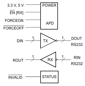
The MAX3221 device consists of one line driver,
one line receiver with dedicated enable pin, and a dual charge-pump circuit with
±15-kV ESD protection pin to pin (serial-port connection pins, including GND). The
device meets the requirements of TIA/EIA-232-F and provides the electrical interface
between an asynchronous communication controller and the serial-port connector. The
charge pump and four small external capacitors allow operation from a single
3-V to 5.5-V supply. These devices operate at data
signaling rates up to 250 kbps and a maximum of 30-V/μs driver output slew rate.
Flexible control options for power management are available when the serial port is inactive. The automatic power-down feature functions when FORCEON is low and
FORCEOFF is high. During this mode of operation, if the device does not sense a valid
RS-232 signal on the receiver input, the driver output is disabled and the supply current is reduced to 1 μA. The
INVALID output notifies the user if an RS-232 signal is present at the receiver input.
| PART NUMBER | PACKAGE(1) | BODY SIZE (NOM) |
|---|---|---|
| MAX3221 | SSOP (DB) (32) | 6.20 mm × 5.30 mm |
| TSSOP (PW) (32) | 5.00 mm × 4.40 mm |
 Simplified Diagram