SLLS636N December 2004 – January 2015 MC33063A , MC34063A
PRODUCTION DATA.
- 1 Features
- 2 Description
- 3 Simplified Schematic
- 4 Revision History
- 5 Pin Configuration and Functions
-
6 Specifications
- 6.1 Absolute Maximum Ratings
- 6.2 ESD Ratings
- 6.3 Recommended Operating Conditions
- 6.4 Thermal Information
- 6.5 Electrical Characteristics—Oscillator
- 6.6 Electrical Characteristics—Output Switch
- 6.7 Electrical Characteristics—Comparator
- 6.8 Electrical Characteristics—Total Device
- 6.9 Typical Characteristics
- 7 Detailed Description
- 8 Application and Implementation
- 9 Power Supply Recommendations
- 10Layout
- 11Device and Documentation Support
- 12Mechanical, Packaging, and Orderable Information
Package Options
Mechanical Data (Package|Pins)
Thermal pad, mechanical data (Package|Pins)
- DRJ|8
Orderable Information
6 Specifications
6.1 Absolute Maximum Ratings
over operating free-air temperature range (unless otherwise noted)(1)| MIN | MAX | UNIT | |||
|---|---|---|---|---|---|
| VCC | Supply voltage | 40 | V | ||
| VIR | Comparator inverting input voltage range | –0.3 | 40 | V | |
| VC(switch) | Switch collector voltage | 40 | V | ||
| VE(switch) | Switch emitter voltage | VPIN1 = 40 V | 40 | V | |
| VCE(switch) | Switch collector to switch emitter voltage | 40 | V | ||
| VC(driver) | Driver collector voltage | 40 | V | ||
| IC(driver) | Driver collector current | 100 | mA | ||
| ISW | Switch current | 1.5 | A | ||
| TJ | Operating virtual junction temperature | 150 | °C | ||
| Tstg | Storage temperature range | –65 | 150 | °C | |
(1) Stresses beyond those listed under Absolute Maximum Ratings may cause permanent damage to the device. These are stress ratings only, and functional operation of the device at these or any other conditions beyond those indicated under Recommended Operating Conditions is not implied. Exposure to absolute-maximum-rated conditions for extended periods may affect device reliability.
6.2 ESD Ratings
| VALUE | UNIT | |||
|---|---|---|---|---|
| V(ESD) | Electrostatic discharge | Human body model (HBM), per ANSI/ESDA/JEDEC JS-001, all pins(1) | 2500 | V |
| Charged device model (CDM), per JEDEC specification JESD22-C101, all pins(2) | 1500 | |||
(1) JEDEC document JEP155 states that 500-V HBM allows safe manufacturing with a standard ESD control process.
(2) JEDEC document JEP157 states that 250-V CDM allows safe manufacturing with a standard ESD control process.
6.3 Recommended Operating Conditions
| MIN | MAX | UNIT | |||
|---|---|---|---|---|---|
| VCC | Supply voltage | 3 | 40 | V | |
| TA | Operating free-air temperature | MC33063A | –40 | 85 | °C |
| MC34063A | 0 | 70 | |||
6.4 Thermal Information
| THERMAL METRIC(1) | MC33063A | UNIT | |||
|---|---|---|---|---|---|
| D | DRJ | P | |||
| 8 PINS | |||||
| RθJA | Junction-to-ambient thermal resistance | 97 | 41 | 85 | °C/W |
(1) For more information about traditional and new thermal metrics, see the IC Package Thermal Metrics application report (SPRA953).
6.5 Electrical Characteristics—Oscillator
VCC = 5 V, TA = full operating range (unless otherwise noted) (see block diagram)| PARAMETER | TEST CONDITIONS | TA | MIN | TYP | MAX | UNIT | |
|---|---|---|---|---|---|---|---|
| fosc | Oscillator frequency | VPIN5 = 0 V, CT = 1 nF | 25°C | 24 | 33 | 42 | kHz |
| Ichg | Charge current | VCC = 5 V to 40 V | 25°C | 24 | 35 | 42 | μA |
| Idischg | Discharge current | VCC = 5 V to 40 V | 25°C | 140 | 220 | 260 | μA |
| Idischg/Ichg | Discharge-to-charge current ratio | VPIN7 = VCC | 25°C | 5.2 | 6.5 | 7.5 | — |
| VIpk | Current-limit sense voltage | Idischg = Ichg | 25°C | 250 | 300 | 350 | mV |
6.6 Electrical Characteristics—Output Switch
VCC = 5 V, TA = full operating range (unless otherwise noted) (see block diagram)(1)| PARAMETER | TEST CONDITIONS | TA | MIN | TYP | MAX | UNIT | |
|---|---|---|---|---|---|---|---|
| VCE(sat) | Saturation voltage – Darlington connection |
ISW = 1 A, pins 1 and 8 connected | Full range | 1 | 1.3 | V | |
| VCE(sat) | Saturation voltage – non-Darlington connection(2) |
ISW = 1 A, RPIN8 = 82 Ω to VCC, forced β ∼ 20 |
Full range | 0.45 | 0.7 | V | |
| hFE | DC current gain | ISW = 1 A, VCE = 5 V | 25°C | 50 | 75 | — | |
| IC(off) | Collector off-state current | VCE = 40 V | Full range | 0.01 | 100 | μA | |
(1) Low duty-cycle pulse testing is used to maintain junction temperature as close to ambient temperature as possible.
(2) In the non-Darlington configuration, if the output switch is driven into hard saturation at low switch currents (≤300 mA) and high driver currents (≥30 mA), it may take up to 2 μs for the switch to come out of saturation. This condition effectively shortens the off time at frequencies ≥30 kHz, becoming magnified as temperature increases. The following output drive condition is recommended in the non-Darlington configuration:
Forced β of output switch = IC,SW / (IC,driver – 7 mA) ≥ 10, where ∼7 mA is required by the 100-Ω resistor in the emitter of the driver to forward bias the Vbe of the switch.
Forced β of output switch = IC,SW / (IC,driver – 7 mA) ≥ 10, where ∼7 mA is required by the 100-Ω resistor in the emitter of the driver to forward bias the Vbe of the switch.
6.7 Electrical Characteristics—Comparator
VCC = 5 V, TA = full operating range (unless otherwise noted) (see block diagram)| PARAMETER | TEST CONDITIONS | TA | MIN | TYP | MAX | UNIT | |
|---|---|---|---|---|---|---|---|
| Vth | Threshold voltage | 25°C | 1.225 | 1.25 | 1.275 | V | |
| Full range | 1.21 | 1.29 | |||||
| ΔVth | Threshold-voltage line regulation | VCC = 5 V to 40 V | Full range | 1.4 | 5 | mV | |
| IIB | Input bias current | VIN = 0 V | Full range | –20 | –400 | nA | |
6.8 Electrical Characteristics—Total Device
VCC = 5 V, TA = full operating range (unless otherwise noted) (see block diagram)| PARAMETER | TEST CONDITIONS | TA | MIN | MAX | UNIT | |
|---|---|---|---|---|---|---|
| ICC | Supply current | VCC = 5 V to 40 V, CT = 1 nF, VPIN7 = VCC, VPIN5 > Vth, VPIN2 = GND, All other pins open |
Full range | 4 | mA | |
6.9 Typical Characteristics
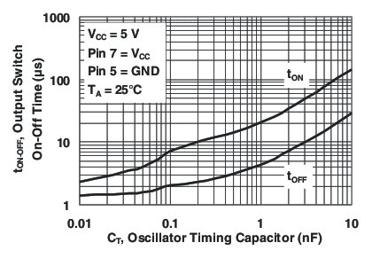 Figure 1. Output Switch On-Off Time vs
Oscillator Timing Capacitor
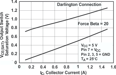 Figure 3. Output Switch Saturation Voltage vs
Collector Current (Common-Emitter Configuration)
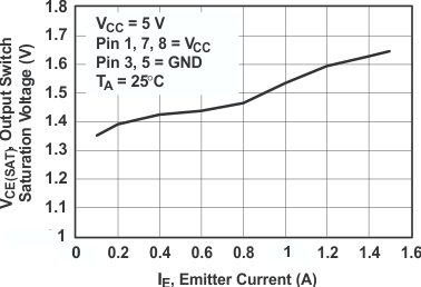 Figure 2. Output Switch Saturation Voltage vs
Emitter Current (Emitter-Follower Configuration)
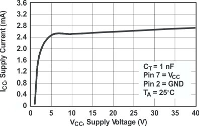 Figure 4. Standby Supply Current vs Supply Voltage