SLASED9C November   2016  – October 2019 MUX36D08 , MUX36S16

PRODUCTION DATA.  

  1. Features
  2. Applications
  3. Description
    1.     Device Images
      1.      Simplified Schematic
      2.      Leakage Current vs Temperature
  4. Revision History
  5. Pin Configuration and Functions
    1.     Pin Functions, MUX36S16
    2.     Pin Functions: MUX36D08
  6. Specifications
    1. 6.1 Absolute Maximum Ratings
    2. 6.2 ESD Ratings
    3. 6.3 Recommended Operating Conditions
    4. 6.4 Thermal Information
    5. 6.5 Electrical Characteristics: Dual Supply
    6. 6.6 Electrical Characteristics: Single Supply
    7. 6.7 Typical Characteristics
  7. Parameter Measurement Information
    1. 7.1 Truth Tables
      1. 7.1.1  On-Resistance
      2. 7.1.2  Off Leakage
      3. 7.1.3  On-Leakage Current
      4. 7.1.4  Differential On-Leakage Current
      5. 7.1.5  Transition Time
      6. 7.1.6  Break-Before-Make Delay
      7. 7.1.7  Turn-On and Turn-Off Time
      8. 7.1.8  Charge Injection
      9. 7.1.9  Off Isolation
      10. 7.1.10 Channel-to-Channel Crosstalk
      11. 7.1.11 Bandwidth
      12. 7.1.12 THD + Noise
  8. Detailed Description
    1. 8.1 Overview
    2. 8.2 Functional Block Diagram
    3. 8.3 Feature Description
      1. 8.3.1 Ultralow Leakage Current
      2. 8.3.2 Ultralow Charge Injection
      3. 8.3.3 Bidirectional Operation
      4. 8.3.4 Rail-to-Rail Operation
    4. 8.4 Device Functional Modes
  9. Application and Implementation
    1. 9.1 Application Information
    2. 9.2 Typical Application
      1. 9.2.1 Design Requirements
      2. 9.2.2 Detailed Design Procedure
      3. 9.2.3 Application Curve
  10. 10Power Supply Recommendations
  11. 11Layout
    1. 11.1 Layout Guidelines
    2. 11.2 Layout Example
  12. 12Device and Documentation Support
    1. 12.1 Documentation Support
      1. 12.1.1 Related Documentation
    2. 12.2 Related Links
    3. 12.3 Receiving Notification of Documentation Updates
    4. 12.4 Community Resources
    5. 12.5 Trademarks
    6. 12.6 Electrostatic Discharge Caution
    7. 12.7 Glossary
  13. 13Mechanical, Packaging, and Orderable Information

Package Options

Mechanical Data (Package|Pins)
Thermal pad, mechanical data (Package|Pins)
Orderable Information

Transition Time

Transition time is defined as the time taken by the output of the MUX36xxx to rise or fall to 90% of the transition after the digital address signal has fallen or risen to 50% of the transition. Figure 30 shows the setup used to measure transition time, denoted by the symbol tt.
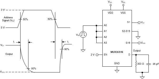
MUX36S16 MUX36D08 trans_time_meas_setup_LASED9.gifFigure 30. Transition-Time Measurement Setup