SLLS910A July 2008 – June 2016 ONET8501PB
PRODUCTION DATA.
- 1 Features
- 2 Applications
- 3 Description
- 4 Revision History
- 5 Description (continued)
- 6 Pin Configuration and Functions
- 7 Specifications
-
8 Detailed Description
- 8.1 Overview
- 8.2 Functional Block Diagram
- 8.3 Feature Description
- 8.4 Device Functional Modes
- 8.5 Programming
- 8.6
Register Maps
- 8.6.1 Register 0 (0x00) Mapping - Control Settings
- 8.6.2 Register 1 (0x01) Mapping - Input Threshold Adjust
- 8.6.3 Register 2 (0x02) Mapping - Preemphasis Adjust
- 8.6.4 Register 3 (0x03) Mapping - Output Amplitude Adjust
- 8.6.5 Register 4 (0x04) Mapping - Rate Selection Register A
- 8.6.6 Register 5 (0x05) Mapping - Rate Selection Register B
- 8.6.7 Register 6 (0x06) Mapping - Rate Selection Register C
- 8.6.8 Register 7 (0x07) Mapping - Rate Selection Register D
- 8.6.9 Register 8 (0x08) Mapping - LOS Assert Level Register A
- 8.6.10 Register 9 (0x09) Mapping - LOS Assert Level Register B
- 8.6.11 Register 10 (0x0A) Mapping - LOS Assert Level Register C
- 8.6.12 Register 11 (0x0B) Mapping - LOS Assert Level Register D
- 8.6.13 Register 14 (0x0E) Mapping - Selected Rate Setting (Read Only)
- 8.6.14 Register 15 (0x0F) Mapping - Selected LOS Level (Read Only)
- 9 Application and Implementation
- 10Power Supply Recommendations
- 11Layout
- 12Device and Documentation Support
- 13Mechanical, Packaging, and Orderable Information
Package Options
Mechanical Data (Package|Pins)
- RGT|16
Thermal pad, mechanical data (Package|Pins)
- RGT|16
Orderable Information
7 Specifications
7.1 Absolute Maximum Ratings
over operating free-air temperature range (unless otherwise noted)(1)| MIN | MAX | UNIT | ||
|---|---|---|---|---|
| VCC | Supply voltage(2) | –0.3 | 4 | V |
| VDIN+, VDIN– | Voltage at DIN+, DIN–(2) | 0.5 | 4 | V |
| VLOS, VCOC1, VCOC2, VDOUT+, VDOUT–, VDIS, VRATE0, VRATE1, VSDA, VSCK | Voltage at LOS, COC1, COC2, DOUT+, DOUT–, DIS, RATE0, RATE1, SDA, SCK(2) | –0.3 | 4 | V |
| VDIN,DIFF | Differential voltage between DIN+ and DIN– | ±2.5 | V | |
| IDIN+, IDIN–, IDOUT+, IDOUT– | Continuous current at inputs and outputs | 25 | mA | |
| TLEAD | Lead temperature 1.6mm (1/16 inch) from case for 10 s | 260 | °C | |
| TA | Characterized free-air operating temperature | –40 | 100 | °C |
| TJ,max | Maximum junction temperature | 125 | °C | |
| Tstg | Storage temperature | –65 | 150 | °C |
(1) Stresses beyond those listed under Absolute Maximum Ratings may cause permanent damage to the device. These are stress ratings only, which do not imply functional operation of the device at these or any other conditions beyond those indicated under Recommended Operating Conditions. Exposure to absolute-maximum-rated conditions for extended periods may affect device reliability.
(2) All voltage values are with respect to network ground terminal.
7.2 ESD Ratings
| VALUE | UNIT | |||
|---|---|---|---|---|
| V(ESD) | Electrostatic discharge | Human-body model (HBM), per ANSI/ESDA/JEDEC JS-001(1) | ±2000 | V |
| Charged-device model (CDM), per JEDEC specification JESD22-C101(2) | ±750 | |||
(1) JEDEC document JEP155 states that 500-V HBM allows safe manufacturing with a standard ESD control process.
(2) JEDEC document JEP157 states that 250-V CDM allows safe manufacturing with a standard ESD control process.
7.3 Recommended Operating Conditions
| MIN | NOM | MAX | UNIT | ||
|---|---|---|---|---|---|
| VCC | Supply voltage | 2.95 | 3.3 | 3.6 | V |
| TA | Operating free-air temperature | –40 | 100 | °C | |
| DIGITAL input high voltage | 2 | V | |||
| DIGITAL input low voltage | 0.8 | V | |||
7.4 DC Electrical Characteristics
Over recommended operating conditions, outputs connected to a 50-Ω load, AMP1 = 0, AMP0 = 1 (Register 3) unless otherwise noted. Typical operating condition is at VCC = 3.3 V and TA = 25°C.| PARAMETER | TEST CONDITIONS | MIN | TYP | MAX | UNIT | |
|---|---|---|---|---|---|---|
| VCC | Supply voltage | 2.95 | 3.3 | 3.6 | V | |
| IVCC | Supply current | DIS = 0, CML currents included | 50 | 63 | mA | |
| RIN | Data input resistance | Differential | 100 | Ω | ||
| ROUT | Data output resistance | Single-ended, referenced to VCC | 50 | Ω | ||
| LOS HIGH voltage | ISOURCE = 50 µA with 10-kΩ pullup to VCC | 2.4 | V | |||
| LOS LOW voltage | ISINK = 10 mA with 10-kΩ pullup to VCC | 0.4 | V | |||
7.5 AC Electrical Characteristics
Over recommended operating conditions, outputs connected to a 50-Ω load, AMP1 = 0, AMP0 = 1 (Register 3) and maximum bandwidth unless otherwise noted. Typical operating condition is at VCC = 3.3 V and TA = 25°C.| PARAMETER | TEST CONDITION | MIN | TYP | MAX | UNIT | |
|---|---|---|---|---|---|---|
| f3dB-H | –3-dB bandwidth default settings | RATE1 = 1, RATE0 = 0 | 7.5 | 9 | GHz | |
| RATE1 = 1, RATE0 = 1 | 8.4 | |||||
| RATE1 = 0, RATE0 = 1 | 7.6 | |||||
| RATE1 = 0, RATE0 = 0 | 2.4 | |||||
| f3dB-L | Low frequency –3-dB bandwidth | With 330-pF COC capacitor | 10 | 45 | kHz | |
| VIN,MIN | Data input sensitivity | PRBS31 pattern at 11.3 Gbps, BER < 10–12 | 5 | 9 | mVpp | |
| VOD-min ≥ 0.95 × VOD (output limited) | 20 | 30 | ||||
| PRBS31 pattern at 8.5 Gbps, BER < 10–12, RATE1 = 1, RATE0 = 0 | 4 | |||||
| PRBS31 pattern at 4.25 Gbps, BER < 10–12, RATE1 = 1, RATE0 = 1 | 4 | |||||
| PRBS31 pattern at 2.125 Gbps, BER < 10–12, RATE1 = 0, RATE0 = 1 | 4 | |||||
| SDD11 | Differential input return gain | 0.01 GHz < f < 3.9 GHz | –16 | dB | ||
| 3.9 GHz < f < 12.1 GHz | See (1) | |||||
| SDD22 | Differential output return gain | 0.01 GHz < f < 3.9 GHz | –16 | dB | ||
| 3.9 GHz < f < 12.1 GHz | See(1) | |||||
| SCD11 | Differential to common-mode conversion gain | 0.01 GHz < f < 12.1 GHz | –15 | dB | ||
| SCC22 | Common-mode output return gain | 0.01 GHz < f < 7.5 GHz | –13 | dB | ||
| 7.5 GHz < f < 12.1 GHz | –9 | |||||
| A | Small signal gain | 29 | 34 | dB | ||
| VIN,MAX | Data input overload | 2000 | mVpp | |||
| DJ | Deterministic jitter at 11.3 Gbps | VIN = 15 mVpp, K28.5 pattern | 3 | 8 | pspp | |
| VIN = 30 mVpp, K28.5 pattern | 3 | 10 | ||||
| VIN = 2000 mVpp, K28.5 pattern | 6 | 15 | ||||
| Deterministic jitter at 8.5 Gbps | VIN = 30 mVpp, K28.5 pattern, RATE1 = 1, RATE0 = 0 | 4 | pspp | |||
| Deterministic jitter at 4.25 Gbps | VIN = 30 mVpp, K28.5 pattern, RATE1 = 1, RATE0 = 1 | 6 | pspp | |||
| Deterministic jitter at 2.125 Gbps | VIN = 30 mVpp, K28.5 pattern, RATE1 = 0, RATE0 = 1 | 8 | pspp | |||
| RJ | Random jitter | VIN = 30 mVpp | 1 | psrms | ||
| VOD | Differential data output voltage | VIN > 30 mVpp, DIS = 0, AMP1 = 0, AMP0 = 0 | 250 | 350 | 450 | mVpp |
| VIN > 30 mVpp, DIS = 0, AMP1 = 0, AMP0 = 1 | 500 | 650 | 800 | |||
| VIN > 30 mVpp, DIS = 0, AMP1 = 1, AMP0 = 1 | 650 | 850 | 1050 | |||
| DIS = 1 | 5 | mVrms | ||||
| VPREEM | Output preemphasis step size | 1 | dB | |||
| tR | Output rise time | 20% to 80%, VIN > 30 mVpp | 28 | 40 | ps | |
| tF | Output fall time | 20% to 80%, VIN > 30 mVpp | 28 | 40 | ps | |
| CMOV | AC common-mode output voltage | PRBS31 pattern; AMP1 = 0, AMP0 = 1 | 7 | mVrms | ||
| VTH | LOW LOS assert threshold range min | K28.5 pattern at 11.3 Gbps, LOSRNG = 0 | 15 | mVpp | ||
| LOW LOS assert threshold range max | K28.5 pattern at 11.3 Gbps, LOSRNG = 0 | 35 | ||||
| VTH | HIGH LOS assert threshold range min | K28.5 pattern at 11.3 Gbps, LOSRNG = 1 | 35 | mVpp | ||
| HIGH LOS assert threshold range max | K28.5 pattern at 11.3 Gbps, LOSRNG = 1 | 80 | ||||
| LOS threshold variation | Versus temperature at 11.3 Gbps | 1.5 | dB | |||
| Versus supply voltage VCC at 11.3 Gbps | 1 | |||||
| Versus data rate | 1.5 | |||||
| LOS hysteresis (electrical) | K28.5 pattern at 11.3 Gbps | 2 | 4 | 6 | dB | |
| TLOS_AST | LOS assert time | 2.5 | 10 | 80 | µs | |
| TLOS_DEA | LOS deassert time | 2.5 | 10 | 80 | µs | |
| TDIS | Disable response time | 20 | ns | |||
(1) Differential Return Gain given by SDD11, SDD22 = –11.6 + 13.33 log10(f/8.25), f in GHz
7.6 Typical Characteristics
Typical operating condition is at VCC = 3.3 V, TA = 25°C, AMP1 = 0, AMP0 = 1 (Register 3), and maximum bandwidth unless otherwise noted.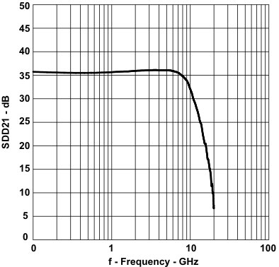 Figure 1. Frequency Response
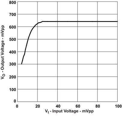 Figure 3. Transfer Function
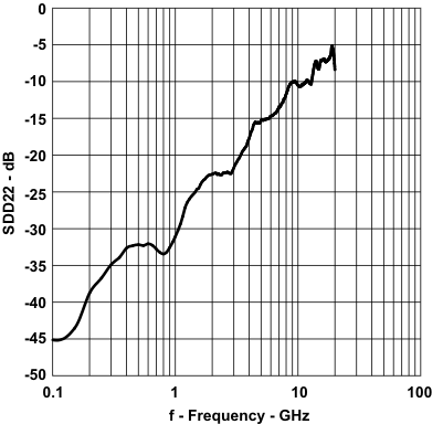 Figure 5. Differential Output Return Gain vs
Frequency
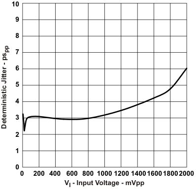 Figure 7. Deterministic Jitter vs
Input Voltage
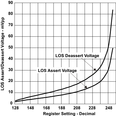 Figure 9. LOS Assert/Deassert Voltage vs
Register Setting LOSRNG = 0
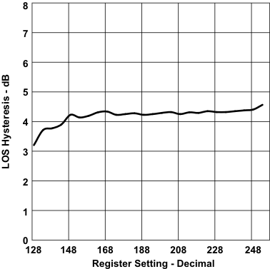 Figure 11. LOS Hysteresis vs
Register Setting LOSRNG = 0
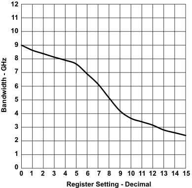 Figure 2. Bandwidth vs Register Setting
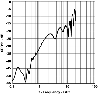 Figure 4. Differential Input Return Gain vs
Frequency
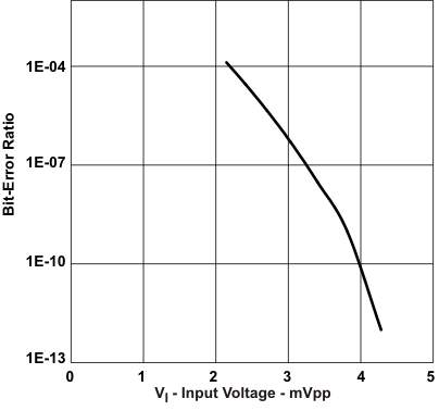 Figure 6. BIT-Error Ratio vs
Input Voltage (11.3 GBPS)
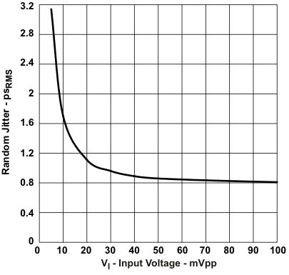 Figure 8. Random Jitter vs
Input Voltage
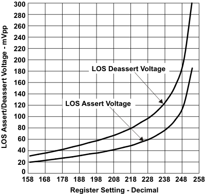 Figure 10. LOS Assert/Deassert Voltage vs
Register Setting LOSRNG = 1
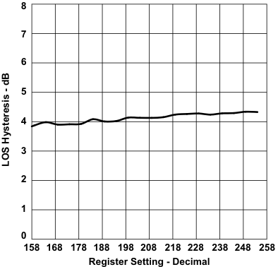 Figure 12. LOS Hysteresis vs
Register Setting LOSRNG = 1