SBOS427F June 2017 – March 2021 OPA145 , OPA2145
PRODUCTION DATA
- 1 Features
- 2 Applications
- 3 Description
- 4 Revision History
- 5 Pin Configuration and Functions
- 6 Specifications
- 7 Detailed Description
- 8 Application and Implementation
- 9 Power Supply Recommendations
- 10Layout
- 11Device and Documentation Support
- 12Mechanical, Packaging, and Orderable Information
Package Options
Mechanical Data (Package|Pins)
Thermal pad, mechanical data (Package|Pins)
- DGK|8
Orderable Information
8.2.2 Detailed Design Procedure
The infinite-gain multiple-feedback circuit for a low-pass network function is shown in Figure 8-1. Use Equation 2 to calculate the voltage transfer function.
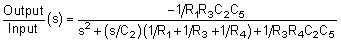
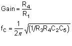
This circuit produces a signal inversion. For this circuit, the gain at dc and the low-pass cutoff frequency are calculated by Equation 3:
For systems which have different filter parameters or require specific system optimization, such as minimizing the system noise, an alternative device may be desired. A list of recommended alternatives can be found in Table 8-1.
| FEATURES | PRODUCT |
|---|---|
| Low-power, 10-MHz FET input industrial op amp | OPA140 |
| 2.2-nV/√ Hz, low-power, 36-V op amp in SOT-23 package | OPA209 |
| Low-noise, high-precision, 22-MHz, 4-nV/√ Hz JFET-input op amp | OPA827 |
| Low-noise, low IQ precision CMOS op amp | OPA376 |
| Low-power, precision, CMOS, rail-to-rail input/output, low-offset, low-bias op amp | OPA191 |
Software tools are readily available to simplify filter design. WEBENCH® Filter Designer is a simple, powerful, and easy-to-use active filter design program. The WEBENCH® Filter Designer lets designers create optimized filter designs using a selection of TI operational amplifiers and passive components from TI's vendor partners.
Available as a web based tool from the WEBENCH Design Center, WEBENCH Filter Designer allows designers to design, optimize, and simulate complete multistage active filter solutions within minutes.