SBOS855E January 2017 – December 2022 OPA1677 , OPA1678 , OPA1679
PRODUCTION DATA
- 1 Features
- 2 Applications
- 3 Description
- 4 Revision History
- 5 Pin Configuration and Functions
- 6 Specifications
- 7 Detailed Description
-
8 Application and Implementation
- 8.1 Application Information
- 8.2 Typical Applications
- 8.3 Power Supply Recommendations
- 8.4 Layout
- 9 Device and Documentation Support
- 10Mechanical, Packaging, and Orderable Information
Package Options
Mechanical Data (Package|Pins)
Thermal pad, mechanical data (Package|Pins)
Orderable Information
8.2.1.2.1 Power Supply
In professional audio systems, phantom power is applied to the two signal lines that carry a differential audio signal from the microphone. Figure 8-2 is a diagram of the system showing 48-V phantom power applied to the differential signal lines between the piezo preamplifier output and the input of a professional microphone preamplifier.
 Figure 8-2 System Diagram Showing the
Application of Phantom Power to the Audio Signal Lines
Figure 8-2 System Diagram Showing the
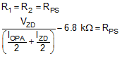
Application of Phantom Power to the Audio Signal LinesA voltage divider is used to extract the common-mode phantom power from the differential audio signal in this type of system. The voltage at center point of the voltage divider formed by R1 and R2 does not change when audio signals are present on the signal lines (assuming R1 and R2 are matched). A Zener diode forces the voltage at the center point of R1 and R2 to a regulated voltage. The values of R1 and R2 are determined by the allowable voltage drop across these resistors from the current delivered to both op amp channels and the Zener diode. There are two power supply current pathways in parallel, each sharing half the total current of the op amp and Zener diode. Resistors R1 and R2 can be calculated using Equation 1:
A 24-V Zener diode is selected for this design, and 1 mA of current flows through the diode at idle conditions to maintain the reverse-biased condition of the Zener diode. The maximum idle power supply current of both op amp channels is 5 mA. Inserting these values into Equation 1 gives the values for R1 and R2 shown in Equation 2.
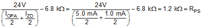
Using a value of 1.2 kΩ for resistors R1 and R2 establishes a 1-mA current through the Zener diode and properly regulate the node to 24 V. Capacitor C1 forms a low-pass filter with resistors R1 and R2 to filter the Zener diode noise and any residual differential audio signals. Mismatch in the values of R1 and R2 causes a portion of the audio signal to appear at the voltage divider center point. The corner frequency of the low-pass filter must be set below the audio band, as shown in Equation 3.
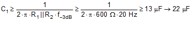
A 22-μF capacitor is selected because the capacitor meets the requirements for power supply filtering and is a widely available denomination. A 0.1-µF capacitor (C2) is added in parallel with C1 as a high-frequency bypass capacitor.