SBOS855E January   2017  – December 2022 OPA1677 , OPA1678 , OPA1679

PRODUCTION DATA  

  1. Features
  2. Applications
  3. Description
  4. Revision History
  5. Pin Configuration and Functions
  6. Specifications
    1. 6.1 Absolute Maximum Ratings
    2. 6.2 ESD Ratings
    3. 6.3 Recommended Operating Conditions
    4. 6.4 Thermal Information: OPA1677
    5. 6.5 Thermal Information: OPA1678
    6. 6.6 Thermal Information: OPA1679
    7. 6.7 Electrical Characteristics
    8. 6.8 Typical Characteristics
  7. Detailed Description
    1. 7.1 Overview
    2. 7.2 Functional Block Diagram
    3. 7.3 Feature Description
      1. 7.3.1 Phase Reversal Protection
      2. 7.3.2 Electrical Overstress
      3. 7.3.3 EMI Rejection Ratio (EMIRR)
        1. 7.3.3.1 EMIRR IN+ Test Configuration
    4. 7.4 Device Functional Modes
      1. 7.4.1 Operating Voltage
  8. Application and Implementation
    1. 8.1 Application Information
      1. 8.1.1 Capacitive Loads
    2. 8.2 Typical Applications
      1. 8.2.1 Phantom-Powered Preamplifier for Piezo Contact Microphones
        1. 8.2.1.1 Design Requirements
        2. 8.2.1.2 Detailed Design Procedure
          1. 8.2.1.2.1 Power Supply
          2. 8.2.1.2.2 Input Network
          3. 8.2.1.2.3 Gain
          4. 8.2.1.2.4 Output Network
        3. 8.2.1.3 Application Curves
      2. 8.2.2 Phono Preamplifier for Moving Magnet Cartridges
      3. 8.2.3 Single-Supply Electret Microphone Preamplifier
      4. 8.2.4 Composite Headphone Amplifier
      5. 8.2.5 Differential Line Receiver With AC-Coupled Outputs
    3. 8.3 Power Supply Recommendations
    4. 8.4 Layout
      1. 8.4.1 Layout Guidelines
        1. 8.4.1.1 Power Dissipation
      2. 8.4.2 Layout Example
  9. Device and Documentation Support
    1. 9.1 Device Support
      1. 9.1.1 Development Support
        1. 9.1.1.1 PSpice® for TI
        2. 9.1.1.2 TINA-TI™ Simulation Software (Free Download)
        3. 9.1.1.3 DIP-Adapter-EVM
        4. 9.1.1.4 DIYAMP-EVM
        5. 9.1.1.5 TI Reference Designs
        6. 9.1.1.6 Filter Design Tool
    2. 9.2 Documentation Support
      1. 9.2.1 Related Documentation
    3. 9.3 Receiving Notification of Documentation Updates
    4. 9.4 Support Resources
    5. 9.5 Trademarks
    6. 9.6 Electrostatic Discharge Caution
    7. 9.7 Glossary
  10. 10Mechanical, Packaging, and Orderable Information

Package Options

Mechanical Data (Package|Pins)
Thermal pad, mechanical data (Package|Pins)
Orderable Information

Application Curves

The frequency response of the preamplifier circuit is shown in Figure 8-3. The –3-dB frequencies are 15.87 Hz and 181.1 kHz, which meet the design requirements. The gain within the passband of the circuit is 18.9 dB, slightly less than the design goal of 20 dB. The reduction in gain is a result of the voltage division between the output resistors of the piezo preamplifier circuit and the input impedance of the microphone preamplifier. The A-weighted noise of the circuit (referred to the input) is 842.2 nVRMS or –119.27 dBu.
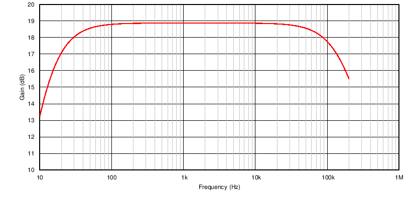
GUID-CF17647E-8B7B-485F-A98D-1FF0E05CBA49-low.pngFigure 8-3 Frequency Response of the Preamplifier Circuit for a 8-nF Piezo Element