SBOS830I September   2017  – October 2021 OPA189 , OPA2189 , OPA4189

PRODUCTION DATA  

  1. Features
  2. Applications
  3. Description
  4. Revision History
  5. Device Comparison Table
  6. Pin Configuration and Functions
  7. Specifications
    1. 7.1 Absolute Maximum Ratings
    2. 7.2 ESD Ratings
    3. 7.3 Recommended Operating Conditions
    4. 7.4 Thermal Information: OPA189
    5. 7.5 Thermal Information: OPA2189
    6. 7.6 Thermal Information: OPA4189
    7. 7.7 Electrical Characteristics
    8. 7.8 Typical Characteristics
  8. Detailed Description
    1. 8.1 Overview
    2. 8.2 Functional Block Diagram
    3. 8.3 Feature Description
      1. 8.3.1 Operating Characteristics
      2. 8.3.2 Phase-Reversal Protection
      3. 8.3.3 Input Bias Current Clock Feedthrough
      4. 8.3.4 EMI Rejection
      5. 8.3.5 EMIRR +IN Test Configuration
      6. 8.3.6 Electrical Overstress
      7. 8.3.7 MUX-Friendly Inputs
      8. 8.3.8 Noise Performance
      9. 8.3.9 Basic Noise Calculations
    4. 8.4 Device Functional Modes
  9. Application and Implementation
    1. 9.1 Application Information
    2. 9.2 Typical Applications
      1. 9.2.1 25-kHz Low-Pass Filter
        1. 9.2.1.1 Design Requirements
        2. 9.2.1.2 Detailed Design Procedure
        3. 9.2.1.3 Application Curve
      2. 9.2.2 Discrete INA + Attenuation for ADC With 3.3-V Supply
      3. 9.2.3 Bridge Amplifier
      4. 9.2.4 Low-Side Current Monitor
      5. 9.2.5 Programmable Power Supply
      6. 9.2.6 RTD Amplifier With Linearization
    3. 9.3 System Examples
      1. 9.3.1 24-Bit, Delta-Sigma, Differential Load Cell or Strain Gauge Sensor Signal Conditioning
  10. 10Power Supply Recommendations
  11. 11Layout
    1. 11.1 Layout Guidelines
    2. 11.2 Layout Example
  12. 12Device and Documentation Support
    1. 12.1 Device Support
      1. 12.1.1 Development Support
        1. 12.1.1.1 TINA-TI™ Simulation Software (Free Download)
        2. 12.1.1.2 TI Precision Designs
    2. 12.2 Documentation Support
      1. 12.2.1 Related Documentation
    3. 12.3 Receiving Notification of Documentation Updates
    4. 12.4 Support Resources
    5. 12.5 Trademarks
    6. 12.6 Electrostatic Discharge Caution
    7. 12.7 Glossary
  13. 13Mechanical, Packaging, and Orderable Information

Package Options

Mechanical Data (Package|Pins)
Thermal pad, mechanical data (Package|Pins)
Orderable Information

Discrete INA + Attenuation for ADC With 3.3-V Supply

Note:

The TINA-TI™ software files shown in the following sections require that either the TINA™ software (from DesignSoft™) or TINA-TI simulation software be installed. See Section 12.1.1.1 for more information.

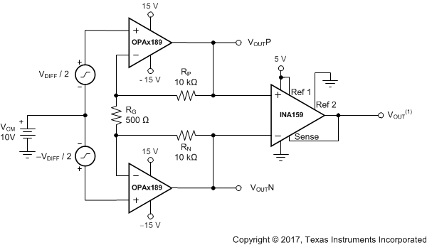
Figure 9-3 shows an example of how the OPAx189 is used as a high-voltage, high-impedance front end for a precision, discrete instrumentation amplifier with attenuation. The INA159 provides the attenuation that allows this circuit to simply interface with 3.3-V or 5-V analog-to-digital converters (ADCs). Click the following link download the TINA-TI software file: Discrete INA.
GUID-88B7BB97-E1D5-4A19-996E-66CD5F4C13E4-low.gif
(1)  VOUT = VDIFF × (41 / 5) + (Ref 1) / 2.
Figure 9-3 Discrete INA + Attenuation for ADC With 3.3-V Supply