SBOS918A March 2018 – January 2021 OPA197-Q1 , OPA2197-Q1 , OPA4197-Q1
PRODUCTION DATA
- 1 Features
- 2 Applications
- 3 Description
- 4 Revision History
- 5 Pin Configuration and Functions
-
6 Specifications
- 6.1 Absolute Maximum Ratings
- 6.2 ESD Ratings
- 6.3 Recommended Operating Conditions
- 6.4 Thermal Information: OPA197-Q1
- 6.5 Thermal Information: OPA2197-Q1
- 6.6 Thermal Information: OPA4197-Q1
- 6.7 Electrical Characteristics: VS = ±4 V to ±18 V (VS = 8 V to 36 V)
- 6.8 Electrical Characteristics: VS = ±2.25 V to ±4 V (VS = 4.5 V to 8 V)
- 6.9 Typical Characteristics
- 7 Detailed Description
- 8 Application and Implementation
- 9 Power Supply Recommendations
- 10Layout
- 11Device and Documentation Support
- 12Mechanical, Packaging, and Orderable Information
Package Options
Mechanical Data (Package|Pins)
- DGK|8
Thermal pad, mechanical data (Package|Pins)
Orderable Information
7.3.6 Common-Mode Voltage Range
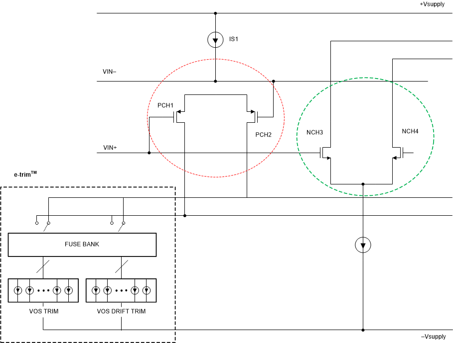
The OPAx197-Q1 are 36-V, true rail-to-rail input operational amplifiers with an input common-mode range that extends 100 mV beyond either supply rail. This wide range is achieved with paralleled complementary N-channel and P-channel differential input pairs, as shown in Figure 7-10. The N-channel pair is active for input voltages close to the positive rail, typically (V+) – 3 V to 100 mV above the positive supply. The P-channel pair is active for inputs from 100 mV below the negative supply to approximately (V+) – 1.5 V. There is a small transition region, typically ( V+) –3 V to (V+) – 1.5 V, in which both input pairs are on. This transition region can vary modestly with process variation, and within this region, PSRR, CMRR, offset voltage, offset drift, noise, and THD performance may be degraded compared to operation outside this region.
 Figure 7-10 Rail-to-Rail Input Stage
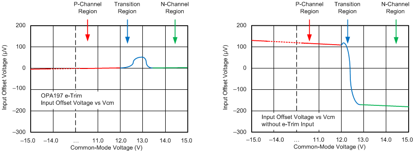
To achieve the best performance for two-stage rail-to-rail input amplifiers, avoid the transition region when possible. The OPAx197-Q1 use a precision trim for both the N-channel and P-channel regions. This technique enables significantly lower levels of offset than previous-generation devices, causing variance in the transition region of the input stages to appear exaggerated relative to offset over the full common-mode range, as shown in Figure 7-11.
 Figure 7-11 Common-Mode Transition vs Standard Rail-to-Rail Amplifiers