SBOS861A June   2017  – June 2018 OPA180-Q1 , OPA2180-Q1

PRODUCTION DATA.  

  1. Features
  2. Applications
  3. Description
    1.     Low Noise (Peak-to-Peak Noise = 250 nV)
  4. Revision History
  5. Device Comparison Table
  6. Pin Configuration and Functions
    1.     Pin Functions: OPA180-Q1
    2.     Pin Functions: OPA2180-Q1
  7. Specifications
    1. 7.1 Absolute Maximum Ratings
    2. 7.2 ESD Ratings
    3. 7.3 Recommended Operating Conditions
    4. 7.4 Thermal Information: OPA180-Q1
    5. 7.5 Thermal Information: OPA2180-Q1
    6. 7.6 Electrical Characteristics: VS = ±2 V to ±18 V (VS = 4 V to 36 V)
    7. 7.7 Typical Characteristics: Table of Graphs
    8. 7.8 Typical Characteristics
  8. Detailed Description
    1. 8.1 Overview
    2. 8.2 Functional Block Diagram
    3. 8.3 Feature Description
      1. 8.3.1 Operating Characteristics
      2. 8.3.2 EMI Rejection
      3. 8.3.3 Phase-Reversal Protection
      4. 8.3.4 Capacitive Load and Stability
      5. 8.3.5 Electrical Overstress
    4. 8.4 Device Functional Modes
  9. Application and Implementation
    1. 9.1 Application Information
    2. 9.2 Typical Applications
      1. 9.2.1 Bipolar ±10-V Analog Output from a Unipolar Voltage Output DAC
        1. 9.2.1.1 Design Requirements
        2. 9.2.1.2 Detailed Design Procedure
          1. 9.2.1.2.1 Component Selection
        3. 9.2.1.3 Application Curves
      2. 9.2.2 Discrete INA + Attenuation
      3. 9.2.3 RTD Amplifier
  10. 10Power Supply Recommendations
  11. 11Layout
    1. 11.1 Layout Guidelines
    2. 11.2 Layout Example
  12. 12Device and Documentation Support
    1. 12.1 Related Links
    2. 12.2 Trademarks
    3. 12.3 Electrostatic Discharge Caution
    4. 12.4 Glossary
  13. 13Mechanical, Packaging, and Orderable Information

Package Options

Mechanical Data (Package|Pins)
Thermal pad, mechanical data (Package|Pins)
Orderable Information

Typical Characteristics

VS = ±18 V, VCM = VS / 2, RLOAD = 10 kΩ connected to VS / 2, and CL = 100 pF, unless otherwise noted.
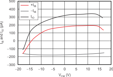
OPA180-Q1 OPA2180-Q1 tc_ib_ios-vcm_bos584.gif
Figure 1. IIB and IIO vs Common-Mode Voltage
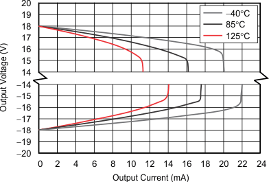
OPA180-Q1 OPA2180-Q1 tc_vo_swing-io_bos584.gif
Figure 3. Output Voltage Swing vs Output Current
(Maximum Supply)
OPA180-Q1 OPA2180-Q1 tc_noise_bos584.gif
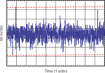
Peak-to-Peak Noise = 250 nV
Figure 5. 0.1-Hz to 10-Hz Noise
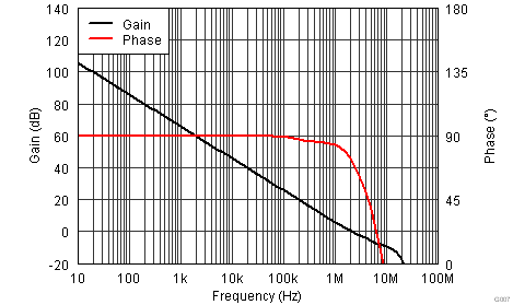
OPA180-Q1 OPA2180-Q1 tc_g_ph-frq_bos525.png
Figure 7. Open-Loop Gain and Phase vs Frequency
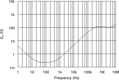
OPA180-Q1 OPA2180-Q1 tc_oloop_iout-frq_bos525.gif
Figure 9. Open-Loop Output Impedance vs Frequency
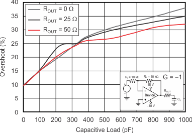
OPA180-Q1 OPA2180-Q1 tc_sm_oshoot-cl_neg_bos584.gif
RL = 10 kΩ
Figure 11. Small-Signal Overshoot vs Capacitive Load
(100-mV Output Step)
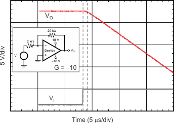
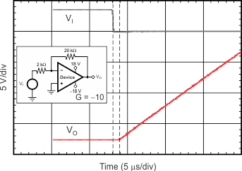
OPA180-Q1 OPA2180-Q1 tc_oload_pos_bos584.gif
Figure 13. Positive Overload Recovery
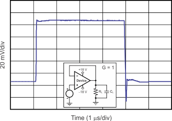
OPA180-Q1 OPA2180-Q1 tc_sm_step_pos_bos584.gif
RL = 10 kΩ CL = 10 pF
Figure 15. Small-Signal Step Response
(100 mV)
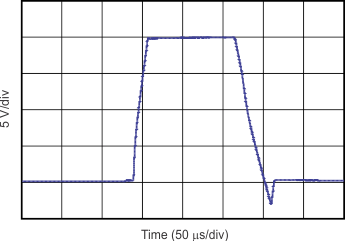
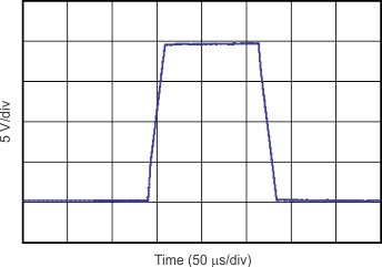
OPA180-Q1 OPA2180-Q1 tc_lg_step_pos_bos584.gif
G = 1 RL = 10 kΩ CL = 10 pF
Figure 17. Large-Signal Step Response
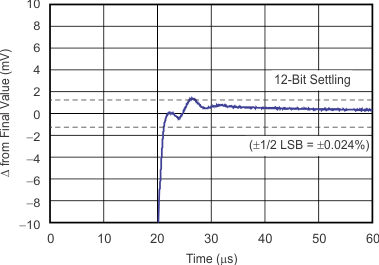
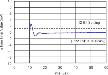
OPA180-Q1 OPA2180-Q1 tc_lg_t_pos_bos584.gif
G = –1
Figure 19. Large-Signal Settling Time (10-V Positive Step)
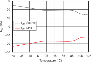
OPA180-Q1 OPA2180-Q1 tc_isc-tmp_bos584.gif
Figure 21. Short-Circuit Current vs Temperature
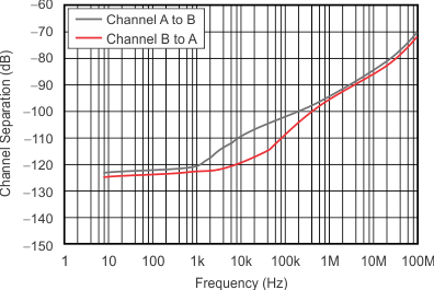
OPA180-Q1 OPA2180-Q1 tc_ch_sep-frq_bos584.gif
Figure 23. Channel Separation vs Frequency
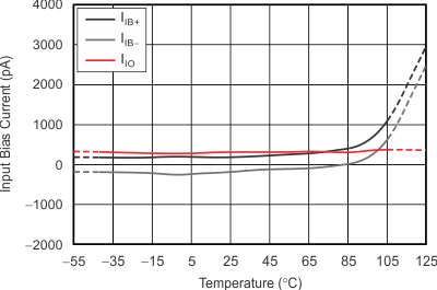
OPA180-Q1 OPA2180-Q1 tc_ibias-tmp_bos584.gif
Figure 2. Input Bias Current vs Temperature
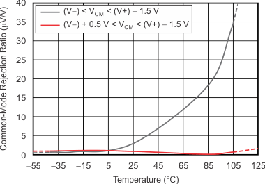
OPA180-Q1 OPA2180-Q1 tc_cmrr-tmp_2v_bos584.gif
VSUPPLY = ±2 V
Figure 4. CMRR vs Temperature
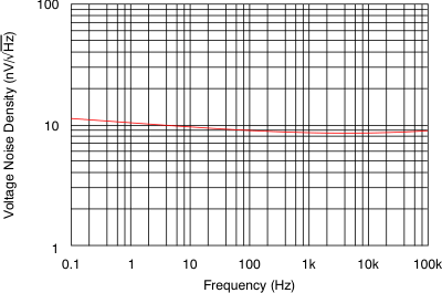
OPA180-Q1 OPA2180-Q1 tc_noise_spec-frq_bos525.gif
Figure 6. Input Voltage Noise Spectral Density vs Frequency
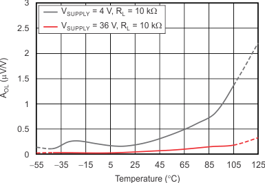
OPA180-Q1 OPA2180-Q1 tc_oloop_g-tmp_bos584.gif
Figure 8. Open-Loop Gain vs Temperature
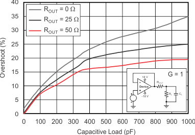
OPA180-Q1 OPA2180-Q1 tc_sm_oshoot-cl_pos_bos584.gif
RL = 10 kΩ
Figure 10. Small-Signal Overshoot vs Capacitive Load
(100-mV Output Step)
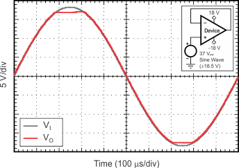
OPA180-Q1 OPA2180-Q1 tc_no_phase_bos584.gif
Figure 12. No Phase Reversal
OPA180-Q1 OPA2180-Q1 tc_oload_neg_bos584.gif
Figure 14. Negative Overload Recovery
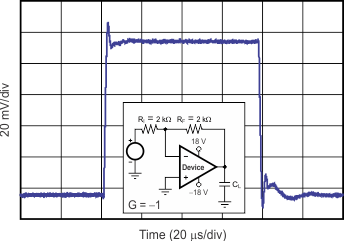
OPA180-Q1 OPA2180-Q1 tc_sm_step_neg_bos584.gif
RL = 10 kΩ CL = 10 pF
Figure 16. Small-Signal Step Response (100 mV)
OPA180-Q1 OPA2180-Q1 tc_lg_step_neg_bos584.gif
G = –1 RL = 10 kΩ CL = 10 pF
Figure 18. Large-Signal Step Response
OPA180-Q1 OPA2180-Q1 tc_lg_t_neg_bos584.gif
G = –1
Figure 20. Large-Signal Settling Time (10-V Negative Step)
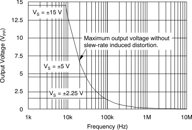
OPA180-Q1 OPA2180-Q1 tc_max_vo-frq_bos525.gif
Figure 22. Maximum Output Voltage vs Frequency
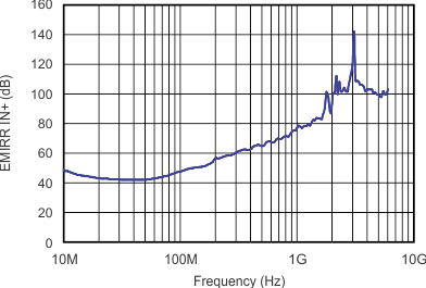
OPA180-Q1 OPA2180-Q1 tc_emirr-frq_bos584.gif
Figure 24. EMIRR IN+ vs Frequency