SBOS525C August 2011 – June 2016 OPA2188
PRODUCTION DATA.
- 1 Features
- 2 Applications
- 3 Description
- 4 Revision History
- 5 Zero-Drift Amplifier Portfolio
- 6 Pin Configuration and Functions
-
7 Specifications
- 7.1 Absolute Maximum Ratings
- 7.2 ESD Ratings
- 7.3 Recommended Operating Conditions
- 7.4 Thermal Information
- 7.5 Electrical Characteristics: High-Voltage Operation, VS = ±4 V to ±18 V (VS = 8 V to 36 V)
- 7.6 Electrical Characteristics: Low-Voltage Operation, VS = ±2 V to < ±4 V (VS = +4 V to < +8 V)
- 7.7 Typical Characteristics: Table of Graphs
- 7.8 Typical Characteristics
- 8 Detailed Description
- 9 Application and Implementation
- 10Power Supply Recommendations
- 11Layout
- 12Device and Documentation Support
- 13Mechanical, Packaging, and Orderable Information
Package Options
Mechanical Data (Package|Pins)
Thermal pad, mechanical data (Package|Pins)
Orderable Information
11 Layout
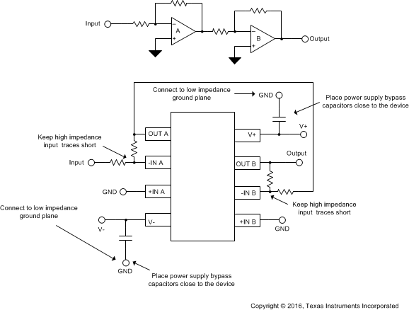
11.1 Layout Guidelines
Pay attention to good layout practices. Keep traces short and when possible, use a printed-circuit-board (PCB) ground plane with surface-mount components placed as close to the device pins as possible. Place a 0.1-μF capacitor closely across the supply pins. Apply these guidelines throughout the analog circuit to improve performance and provide benefits, such as reducing the electromagnetic interference (EMI) susceptibility.
Operational amplifiers vary in susceptibility to radio frequency interference (RFI). RFI can generally be identified as a variation in offset voltage or DC signal levels with changes in the interfering RF signal. The OPA2188 is specifically designed to minimize susceptibility to RFI and demonstrates remarkably low sensitivity compared to previous generation devices. Strong RF fields may still cause varying offset levels.
11.2 Layout Example
 Figure 48. Layout Example