SBOS918A March 2018 – January 2021 OPA197-Q1 , OPA2197-Q1 , OPA4197-Q1
PRODUCTION DATA
- 1 Features
- 2 Applications
- 3 Description
- 4 Revision History
- 5 Pin Configuration and Functions
-
6 Specifications
- 6.1 Absolute Maximum Ratings
- 6.2 ESD Ratings
- 6.3 Recommended Operating Conditions
- 6.4 Thermal Information: OPA197-Q1
- 6.5 Thermal Information: OPA2197-Q1
- 6.6 Thermal Information: OPA4197-Q1
- 6.7 Electrical Characteristics: VS = ±4 V to ±18 V (VS = 8 V to 36 V)
- 6.8 Electrical Characteristics: VS = ±2.25 V to ±4 V (VS = 4.5 V to 8 V)
- 6.9 Typical Characteristics
- 7 Detailed Description
- 8 Application and Implementation
- 9 Power Supply Recommendations
- 10Layout
- 11Device and Documentation Support
- 12Mechanical, Packaging, and Orderable Information
Package Options
Mechanical Data (Package|Pins)
- DGK|8
Thermal pad, mechanical data (Package|Pins)
Orderable Information
3 Description
The OPAx197-Q1 family (OPA197-Q1, OPA2197-Q1, and OPA4197-Q1) is part of a new generation of 36-V, e-trim™ operational amplifiers. The OPAx197-Q1 family of e-trim operational amplifiers uses a proprietary method of package-level trim for offset and offset temperature drift implemented during the final steps of manufacturing after the plastic molding process. This method minimizes the influence of inherent input transistor mismatch, as well as errors induced during package molding.
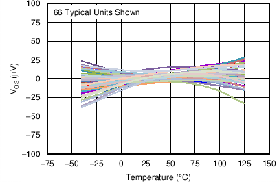
These devices offer outstanding dc precision and ac performance, including rail-to-rail input/output, low offset (±5 µV, typical), low offset drift (±0.2 µV/°C, typical), and a 10-MHz bandwidth.
Unique features such as differential input-voltage range to the supply rail, high output current (±65 mA), high capacitive load drive of up to 1 nF, and high slew rate (20 V/µs) make the OPAx197-Q1 robust, high-performance op amps for high-voltage industrial applications.
| PART NUMBER | PACKAGE(1) | BODY SIZE (NOM) |
|---|---|---|
| OPA197-Q1 | VSSOP (8) | 3.00 mm × 3.00 mm |
| OPA2197-Q1 | ||
| OPA4197-Q1 | TSSOP (14) | 5.00 mm × 4.40 mm |
 The OPAx197-Q1 Maintains
Ultra-Low Input Offset Voltage Over Temperature