SBOS110C May 1998 – March 2023 OPA2227 , OPA2228 , OPA227 , OPA228 , OPA4227 , OPA4228
PRODUCTION DATA
- 1 Features
- 2 Applications
- 3 Description
- 4 Revision History
- 5 Pin Configuration and Functions
-
6 Specifications
- 6.1 Absolute Maximum Ratings
- 6.2 ESD Ratings
- 6.3 Recommended Operating Conditions
- 6.4 Thermal Information: OPA227, OPA228
- 6.5 Thermal Information: OPA2227, OPA2228
- 6.6 Thermal Information: OPA4227, OPA4228
- 6.7 Electrical Characteristics: OPAx227
- 6.8 Electrical Characteristics: OPAx228
- 6.9 Typical Characteristics
- 7 Detailed Description
-
8 Application and Implementation
- 8.1 Application Information
- 8.2 Typical Application
- 8.3 Power Supply Recommendations
- 8.4 Layout
- 9 Device and Documentation Support
- 10Mechanical, Packaging, and Orderable Information
Package Options
Mechanical Data (Package|Pins)
Thermal pad, mechanical data (Package|Pins)
- D|8
Orderable Information
7.3.4 Input Protection
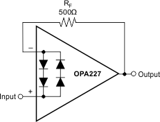
Back-to-back diodes (see Figure 7-2) are used for input protection on the OPAx22x. Exceeding the turn-on threshold of these diodes, as in a pulse condition, can cause current to flow through the input protection diodes as a result of the amplifier finite slew rate. Without external current limiting resistors, the input devices can be destroyed. Sources of high-input current can cause subtle damage to the amplifier. Although the unit can still be functional, important parameters such as input offset voltage, drift, and noise can shift.
 Figure 7-2 Pulsed Operation
When using the OPA227 as a unity-gain buffer (follower), limit the input current to 20 mA. This limiting is accomplished by inserting a feedback resistor or a resistor in series with the source. Equation 1 calculates the sufficient resistor size.
where
- RX is either in series with the source or inserted in the feedback path.
For example, a 10-V pulse (VS = 10 V) requires a total loop resistance of 500 Ω. If the source impedance is large enough to sufficiently limit the current, no additional resistors are needed. Carefully choose the size of any external resistors because of increased noise. For further information on noise calculation, see Section 7.3.6. Figure 7-2 shows an example implementing a current limiting feedback resistor.