SBOS365G may 2006 – may 2023 OPA2365 , OPA365
PRODUCTION DATA
- 1
- 1 Features
- 2 Applications
- 3 Description
- 4 Revision History
- 5 Device Comparison Table
- 6 Pin Configuration and Functions
- 7 Specifications
- 8 Detailed Description
- 9 Application and Implementation
- 10Device and Documentation Support
- 11Mechanical, Packaging, and Orderable Information
Package Options
Mechanical Data (Package|Pins)
- D|8
Thermal pad, mechanical data (Package|Pins)
Orderable Information
9.3.1 Driving an Analog-to-Digital Converter
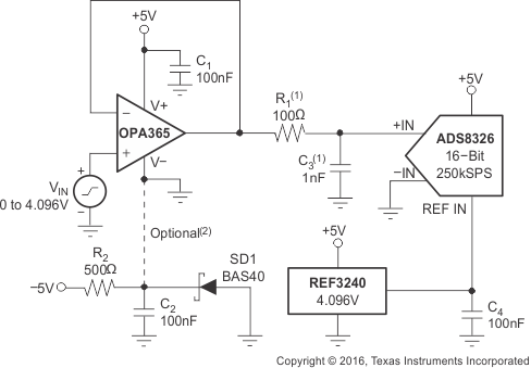
Very wide common-mode input range, rail-to-rail input and output voltage capability, and high speed make the OPAx365 excellent drivers for modern ADCs. Also, because the OPAx365 are free of the input offset transition characteristics inherent to some rail-to-rail CMOS op amps, these devices provide low THD and excellent linearity throughout the input voltage swing range.
Figure 9-5 shows the OPA365 driving an ADS8326, 16-bit, 250-kSPS converter. The amplifier is connected as a unity-gain, noninverting buffer and has an output swing to 0 V, making these devices directly compatible with the ADC minus full-scale input level. The 0-V level is achieved by powering the OPA365 V− pin with a small negative voltage established by the diode forward voltage drop. A small, signal-switching diode or Schottky diode provides a negative supply voltage of −0.3 V to −0.7 V. The supply rail-to-rail is equal to V+, plus the small negative voltage.

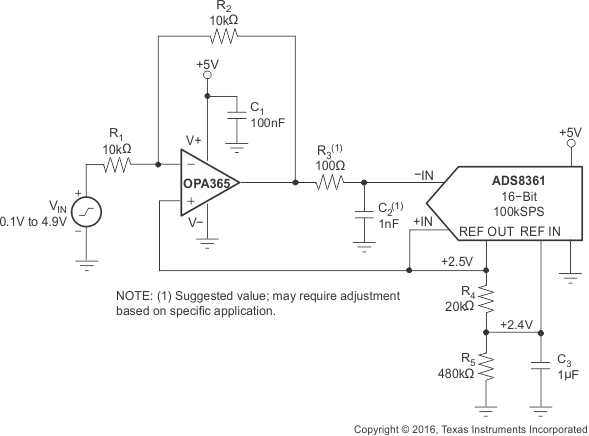
One method to drive an ADC that negates the need for an output swing down to 0 V uses a slightly compressed ADC full-scale input range (FSR). For example, Figure 9-6 shows that the 16-bit ADS8361 has a maximum FSR of 0 V to 5 V when powered by a 5-V supply and VREF of 2.5 V. The idea is to match the ADC input range with the op-amp full-linear output-swing range; for example, an output range of 0.1 V to 4.9 V. The reference output from the ADS8361 ADC is divided down from 2.5 V to 2.4 V using a resistive divider. The ADC FSR then becomes 4.8 VPP centered on a common-mode voltage of 2.5 V. Current from the ADS8361 reference pin is limited to approximately ±10 μA. Here, 5 μA is used to bias the divider. The resistors must be precise to maintain the ADC gain accuracy. An additional benefit of this method is the elimination of the negative supply voltage; these devices require no additional power-supply current.
 Figure 9-6 Driving
the ADS8361
Figure 9-6 Driving
the ADS8361A resistor-capacitor (RC) network, consisting of R1 and C1, is included between the op amp and the ADS8361. The RC network not only provides a high-frequency filter function, but more importantly serves as a charge reservoir used for charging the converter internal hold capacitance. This capability maintains the op-amp output linearity as the ADC input characteristics change throughout the conversion cycle. Depending on the particular application and ADC, some optimization of the R1 and C1 values can be required for best transient performance.
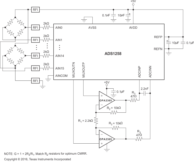
Figure 9-7 illustrates the OPA2365 dual op amp providing signal conditioning within an ADS1258 bridge sensor circuit. The OPA2365 is connected as a differential-in and differential-out amplifier after the ADS1258 16:1 multiplexer. The voltage gain for this stage is approximately 10 V/V. Driving the ADS1258 internal ADC in differential mode, rather than in a single-ended mode, exploits the full linearity performance capability of the converter. For best common-mode rejection, the two R2 resistors must be closely matched.
Note that in Figure 9-7, the amplifiers, bridges, ADS1258, and internal reference are powered by the same single 5-V supply. This ratiometric connection helps cancel excitation voltage drift effects and noise. For best performance, the 5-V supply must be as free as possible from noise and transients.
When the ADS1258 data rate is set to maximum and the chop feature is enabled, this circuit yields 12 bits of noise-free resolution with a 50-mV full-scale input.
The chop feature is used to reduce the ADS1258 offset and offset drift to very low levels. A 2.2-nF capacitor is required across the ADC inputs to bypass the sampling currents. The 47-Ω resistors provide isolation for the OPA2365 outputs from the relatively large, 2.2-nF capacitive load.
 Figure 9-7 Conditioning Input Signals to the ADS1258 on a Single Supply